
Process for preparing tin oxide nanocrystalline thin films

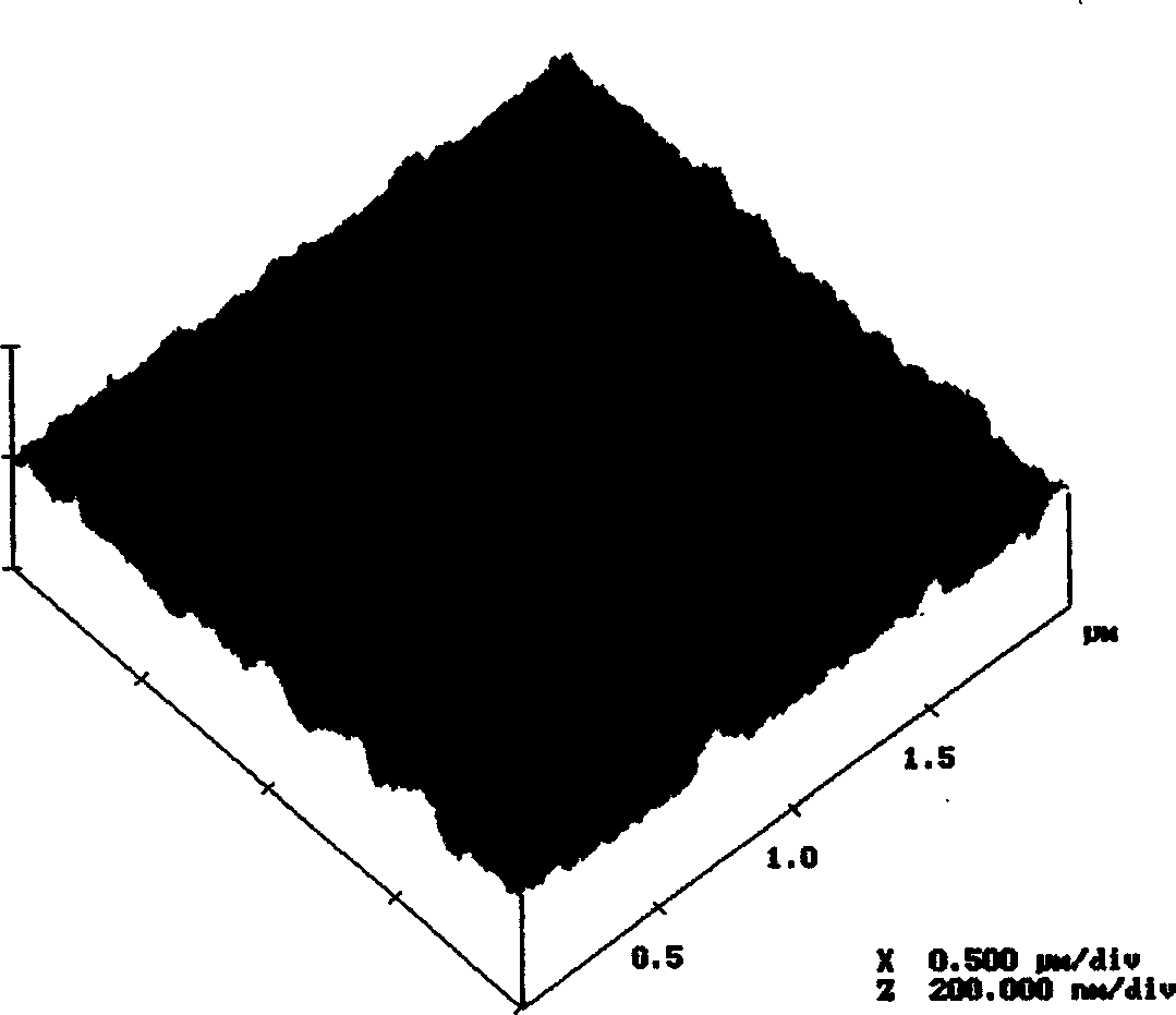
A technology of tin dioxide and nanocrystals, which is applied in semiconductor/solid-state device manufacturing, liquid chemical plating, coating, etc., can solve the problems of high preparation cost, complicated technical process, and large energy consumption, and achieve a dense and uniform film surface , broad application prospects, strong adhesion effect

Inactive Publication Date: 2004-11-10
TIANJIN UNIV
View PDF0 Cites 12 Cited by
  • Summary
  • Abstract
  • Description
  • Claims
  • Application Information

AI Technical Summary

Problems solved by technology

At present, the commonly used methods for preparing tin dioxide thin films include evaporation technology, sputtering technology and chemical vapor deposition technology. At present, the sol-gel technology, which is widely used to prepare various semiconductor ceramic thin films, requires a high-temperature calcination process to perform subsequent heat treatment on the thin film to remove organic solvents and organic templates, so that the thin film can be crystallized.

Method used


Image

  • Process for preparing tin oxide nanocrystalline thin films
  • Process for preparing tin oxide nanocrystalline thin films
  • Process for preparing tin oxide nanocrystalline thin films

Examples


Embodiment 1

[0018] Place the single crystal silicon in distilled water and absolute ethanol for ultrasonic cleaning to wash away the floating dust and organic impurities on the surface; place the clean surface of the single crystal silicon wafer in a mixed solution of concentrated sulfuric acid and hydrogen peroxide with a volume ratio of 3:1 Medium immersion treatment, soaking at 80°C for 20 minutes, the treated substrate was washed with deionized water and isopropanol respectively, blown dry under nitrogen atmosphere, and vacuum dried at 100°C for 40 minutes; use 6.5×10 -3 The anhydrous cyclohexane solution of M mercaptopropyltrimethoxysilane soaked the treated substrate for 30 minutes, washed it with chloroform and deionized water successively after taking it out, and purged and dried it under nitrogen; then put the treated substrate in a volume ratio Soak in a 1:5 solution of hydrogen peroxide and acetic acid at 40°C for 60 minutes; then rinse the substrate with deionized water and chl...

Embodiment 2

[0020] Put the glass in distilled water and acetone and ultrasonically wash it to wash away the floating dust and organic impurities on the surface; put the clean glass piece in the mixed solution of concentrated sulfuric acid and hydrogen peroxide with a volume ratio of 2:1 for soaking treatment at 85°C After soaking for 40 minutes, the treated substrate was washed with deionized water and isopropanol respectively, dried in a helium atmosphere, and vacuum-dried at 90°C for 10 minutes; with 1×10 -3 The benzene solution of M-mercaptododecyltrimethoxysilane soaks the treated substrate for 1 hour, washes it with chloroform and deionized water successively after taking it out, and blows and dries it under helium; then put the treated substrate in a volume ratio of soak in a 1:3 hydrogen peroxide and acetic acid solution at 50°C for 5 minutes; then rinse the substrate with deionized water and chloroform, and dry it with helium. Finally put that base into a 2×10 -3 M SnCl4 / 0.2M HC...

Embodiment 3

[0022] Put alumina as the substrate in distilled water for ultrasonic cleaning to wash away the floating dust and organic impurities on the surface; put the clean alumina substrate in a mixed solution of concentrated sulfuric acid and hydrogen peroxide with a volume ratio of 1.5:1 for soaking treatment , soaked at 95°C for 25 minutes, the treated substrate was washed with deionized water and isopropanol respectively, dried under argon atmosphere, and vacuum-dried at 120°C for 20 minutes; -2 Soak the substrate in toluene solution of M vinyltrimethoxysilane for 2 hours, wash it with chloroform and deionized water in turn after taking it out, and blow and dry it under argon; then place the treated substrate in saturated potassium hydrogen persulfate solution immersion at 50°C for 5 minutes; then the substrate was rinsed with deionized water and chloroform, and dried with argon. Finally put that base into a 3.5×10 -2 M SnCl 4 / 0.6M HCl solution for 3 days, with a pH value of 0.9...


PUM


Abstract

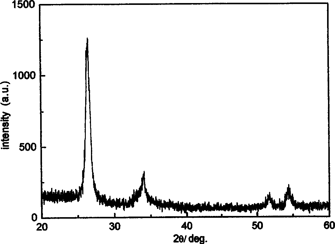
The invention discloses a stannum dioxide nano crystal state film preparing method, including the following steps; (1) washing the surface of a substrate; (2) placing the substrate in the mixed solution of oil of vitriol and oxydol to hydroxylate the surface; (3) dipping the substrate X(CH2)nSi(OH3)3, X(CH2)nSiCl3 or HS(CH2 m solution for soaking, so as to form an organic molecular self-composing single-layer film on the surface; (4) soaking the substrate with mercaptoand alkyl groups as head groups by the mixed solution of oxydol and acetic acid; or soaking the substrate with ethylene as head group by saturated potassium monopersulfate solution, so as to functionalize organic molecular self-composing layer on the surface; (5) dipping the substrate in SnCl4 HCl solution or SnF2 boric acid solution to make a stannum dioxide nano crystal state film. It provides a functionalized surface liquid-phase deposition technique and the prepared products have rutile crystal shaped structure.

Description

technical field [0001] The invention relates to a preparation method of an inorganic nanometer material, in particular to a preparation method of a tin dioxide crystalline thin film. Background technique [0002] As an important functional semiconductor ceramic, tin dioxide can be used to prepare various functional elements such as gas sensitive elements, transparent conductive films, and heat reflective materials. At present, the commonly used methods for preparing tin dioxide thin films include evaporation technology, sputtering technology and chemical vapor deposition technology. At present, the sol-gel technology, which is widely used to prepare various semiconductor ceramic thin films, requires a high-temperature calcination process to perform subsequent heat treatment on the thin film to remove organic solvents and organic templates and crystallize the thin film, although the operation process is simple. Co...

Claims


Application Information

Patent Timeline
IPC IPC(8): C03C17/25C23C18/12H01L21/36
Inventor 张金利李韡翟怡韩永才王素梅王一平袁兵
Owner TIANJIN UNIV
Learn More