Group III nitride compound semiconductor thin film and deposition method thereof, and semiconductor device and manufacturing method thereof

a technology of nitride compound and thin film, which is applied in the direction of vacuum evaporation coating, semiconductor lasers, natural mineral layered products, etc., can solve the problems of limited material and substrate use, difficult to form single-crystal thin films of excellent crystalline, and difficult to uniformly form thin films

Inactive Publication Date: 2003-02-27
MITAMURA SATOSHI
View PDF0 Cites 33 Cited by
  • Summary
  • Abstract
  • Description
  • Claims
  • Application Information

AI Technical Summary

Benefits of technology

[0014] A second object of the invention is to provide a Group III nitride compound semiconductor thin film of uniform film quality and excellent crystalline and a deposition method thereof, and a semiconductor device using such a Group III nitride compound semiconductor and a manufacturing method thereof.

Problems solved by technology

Thus, MBE has a difficulty in forming a thin film of uniform composition and film thickness.
This makes it difficult to form a single-crystal thin film of excellent crystalline.
MOCVD, however, has a problem of the limited material and size of a substrate used.
Thus, sapphire substrates have a problem in workability or formability, resulting in high materials cost.
Another problem with sapphire substrates is low production efficiency.
Since it is difficult to deposit a thin film of uniform film thickness over the entire surface of a substrate, a substrate of large surface area cannot be used (with the current state of art, the maximum size is about 8 inches).
The use of such a single-crystal Group III nitride compound semiconductor thin film as a luminescent material in an LED causes an increase in non-radiative recombination probability in which electrons recombine with holes without emitting radiation, resulting in a problem of deterioration in light emission efficiency.
Secondly, when producing a Group III nitride compound semiconductor comprising gallium as a Group III element, the use of a gallium metal target as a single substance target causes a problem that gallium sputtered from the target becomes attached to and diffused into the inside surfaces of the vacuum chamber 13 to cause corrosion of the vacuum chamber 13.
If the deposition rate is smaller than 15 nm / hour, RF power is too small and the plazma becomes unstable.
This results in deterioration in the crystalline of the poly-crystalline Group III nitride compound semiconductor thin film.
This thin film is so fragile that it is crushed in the scratch test.
If a nitrogen content in the thin film is low, the thin film becomes deficient in nitrogen in the neighborhood of its surface, and the crystalline of the thin film deteriorates while the resistivity of the thin film rapidly increases.

Method used


Image

  • Group III nitride compound semiconductor thin film and deposition method thereof, and semiconductor device and manufacturing method thereof
  • Group III nitride compound semiconductor thin film and deposition method thereof, and semiconductor device and manufacturing method thereof
  • Group III nitride compound semiconductor thin film and deposition method thereof, and semiconductor device and manufacturing method thereof

Examples


example 1

[0074] First, a clear substrate made of cultured quartz having translucency was prepared. The dimensions of the clear substrate, i.e., length, width and height, were 125 mm, 125 mm and 1 mm, respectively. The clear substrate was cleaned with a neutral detergent, washed in water, and then subjected to ultrasonic cleaning with an organic solvent.

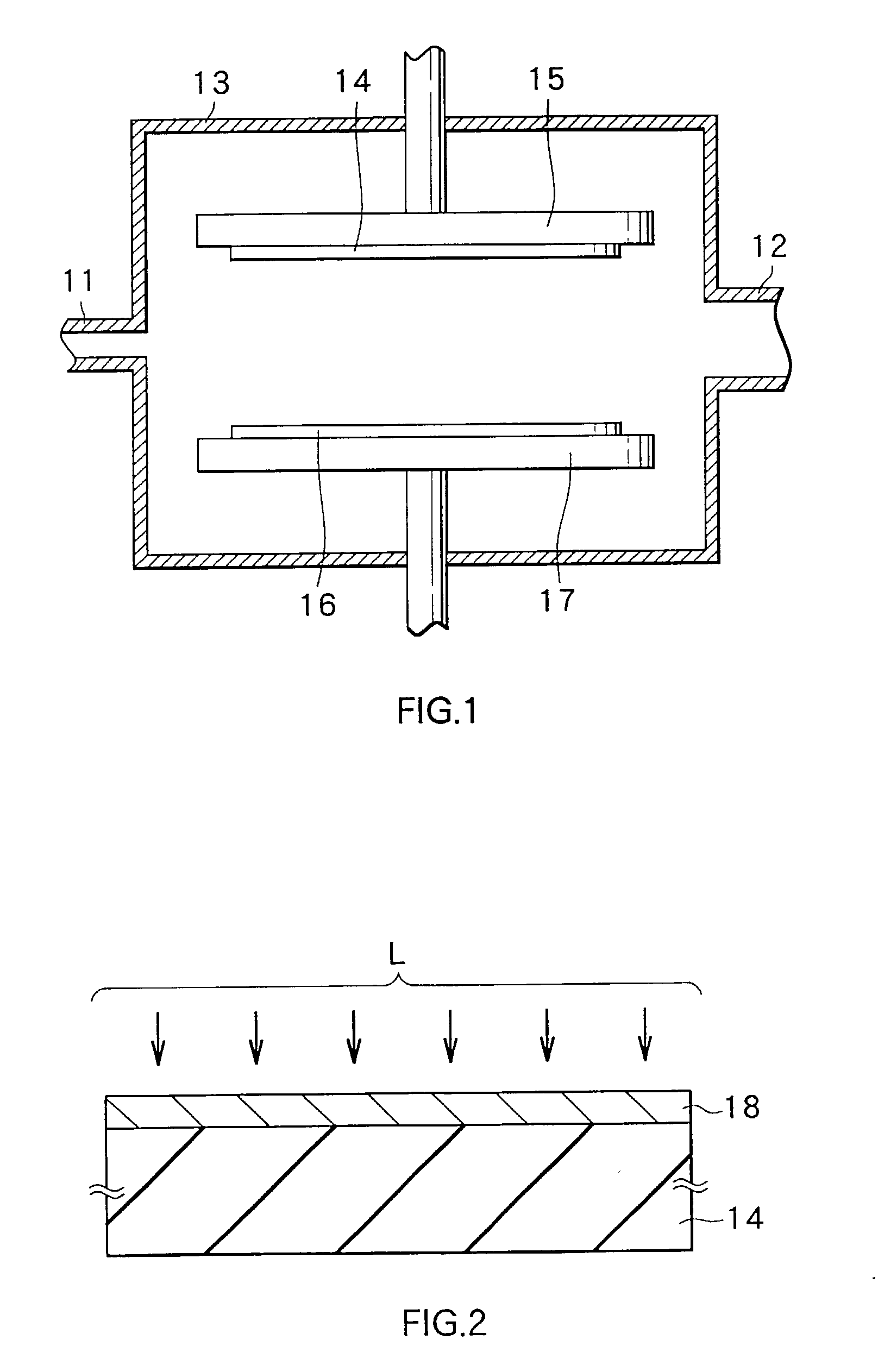
[0075] Then, the clear substrate was mounted on the substrate holder 15 of a sputtering system similar to the sputtering system shown in FIG. 1. Subsequently, a GaN target, i.e., the target 16, in the form of disk 3 inches in diameter and 5 mm in thickness was prepared. The GaN target was mounted on the target mounting plate 17. The distance between the clear substrate and the GaN target was set at 150 mm.

[0076] Next, the gas in the vacuum chamber 13 was exhausted via the gas exhaust pipe 12, and thereby the pressure in the vacuum chamber 13 was reduced to a pressure of 5.0.times.10.sup.-7 Torr. Subsequently, the clear substrate was heated to ...

example 2

[0078] A GaN thin film having a film thickness of 0.1 .mu.m was obtained as in Example 1 except that the RF power was 20 W and sputtering time was 180 minutes. The deposition rate was therefore 33.3 nm / hour.

example 3

[0079] A GaN thin film having a film thickness of 0.1 .mu.m was obtained as in Example 1 except that the RF power was 30 W and sputtering time was 120 minutes. The deposition rate was therefore 50 nm / hour.


PUM

PropertyMeasurementUnit
thicknessaaaaaaaaaa
melting pointaaaaaaaaaa
pressureaaaaaaaaaa

Abstract

A Group III nitride compound semiconductor thin film which can be deposited on any given substrate to have uniform film quality and excellent crystalline, and a deposition method thereof. A semiconductor device and a manufacturing method thereof. A poly-crystalline Group III nitride compound thin film is deposited on a substrate by sputtering at a deposition rate of 15 to 200 nm / hour using a Group III nitride compound target in a plazma atmosphere of gas comprising 10 mole % or more nitrogen. Then, the poly-crystalline Group III nitride compound semiconductor thin film deposited on the substrate is irradiated with an excimer pulsed laser with an energy density of about 200 mJ / cm2, in an atmosphere of gas with an oxygen content of 2 mole % or less. Thereby, lattice defects such as grain boundaries or dislocations which occur in the thin film are removed.

Description

[0001] 1. Field of the Invention[0002] The present invention relates to a Group III nitride compound semiconductor thin film comprising a Group III element such as aluminum (Al), gallium (Ga), indium (In) or boron (B), and nitrogen (N), and a deposition method thereof. The present invention also relates to a semiconductor device comprising such a Group III nitride compound semiconductor thin film, and a manufacturing method thereof[0003] 2. Description of the Related Art[0004] GaN (gallium nitride), InGaN (indium gallium nitride) compound crystal, GaAlN (gallium aluminum nitride) compound crystal and InAlGaN (indium aluminum gallium nitride) compound crystal are typical Group III nitride compound semiconductors. Group III nitride compound semiconductors are attractive as practical semiconductor materials applicable to light emitting devices such as a light emitting diode (LED) that emits blue light or a laser diode (LD) that emits blue light. Active exercise of research and developm...

Claims


Application Information

Patent Timeline
Patent Type & Authority Applications(United States)
IPC IPC(8): B32B9/00C23C14/06H01L21/20H01L21/203H01L21/205H01L21/268H01L21/31H01L33/32H01S5/323
CPCC23C14/0617H01L33/007H01L21/0237H01L21/02458H01L21/0254H01L21/02576H01L21/0262H01L21/02631H01L21/0242
Inventor MITAMURA, SATOSHI
Owner MITAMURA SATOSHI
Why Eureka
Try Eureka