Fluorination treatment apparatus, process for producing fluorination treated substance, and fluorination treated substance

a technology of treatment apparatus and treatment substance, which is applied in the direction of solid-state diffusion coating, halogenated hydrocarbon preparation, organic chemistry, etc., can solve the problems of unable to achieve the desired image formation performance, and prolonging the exposure time. , to achieve the effect of enhancing the transmittance in the vacuum ultraviolet region and reducing the fluorine deficiency of a substan

Inactive Publication Date: 2004-01-08
SHOWA DENKO KK +1
View PDF8 Cites 34 Cited by
  • Summary
  • Abstract
  • Description
  • Claims
  • Application Information

AI Technical Summary

Benefits of technology

[0026] It is a first object of the present invention to provide a fluorination treatment apparatus capable of remarkably reducing fluorine deficiency of a substance to be treated, such as a fluoride thin film, to enhance transmittance in the vacuum ultraviolet region, a process for producing a fluorination treated substance, and a fluorination treated substance obtained by the process.
[0027] It is a second object of the present invention to provide a process for producing a fluoride optical element, wherein trace amounts of abrasive grains sticking into the abraded surface of the fluoride optical element and a work-modification layer formed on the surface are removed to obtain a fluoride optical element reduced in the small light absorption loss and having a smooth and clean surface, and a fluoride optical element obtained by the process.
[0032] According to the fluorination treatment apparatus as stated in (1) or (2), fluorine deficiency of the substance to be treated can be compensated by carrying out the fluorination treatment. Further, not only the fluorine deficiency of the substance to be treated can be compensated but-also impurities are decreased, whereby the substance to be treated can be converted into a fluoride of stoichiometric composition. Hence, light absorption loss in the vacuum ultraviolet region and the ultraviolet region can be reduced. By carrying out the fluorination treatment, furthermore, crystalline properties of the substance to be treated can be enhanced and the structural defects can be decreased. By carrying out the fluorination treatment, moreover, laser beam resistance of the substance to be treated can be enhanced.
[0078] In the fluorination treated substances as stated in (23) to (26), namely, fluoride thin film, fluoride powder, fluoride solid and fluoride optical element, the fluorine deficiency has been compensated and the impurities have been decreased, that is, the substances have been converted into fluorides of stoichiometric composition. Hence, light absorption loss in the vacuum ultraviolet region and the ultraviolet region can be reduced. In these substances, further, the crystalline properties have been enhanced, the structural defects have been decreased, and the laser beam resistance has been enhanced.

Problems solved by technology

The reason why the thin film must be formed only by heating the optical element as a substrate at a relatively low temperature is that high-temperature heating causes thermal deformation of the optical element to thereby produce deviation of the dimensional accuracy of the optical element surface, so that desired performance of image formation cannot be obtained.
Consequently, the exposure time is prolonged, and the productivity becomes extremely bad.
Further, a fluorine-deficient fluoride thin film or a fluorine-deficient and oxygen-containing fluoride thin film has poor laser beam resistance because such a film contains structural defects or impurities, and hence the optical element parts need to be changed frequently to further deteriorate productivity of the exposure apparatus.
Under such circumstances, the present inventors have earnestly studied, and as a result, they have found that when the fluoride optical element for the vacuum ultraviolet light of shorter wavelength is subjected to conventional cleaning after the precision abrasion (final abrasion), there is a new problem peculiar to the fluoride optical element obtained by the surface abrasion.
By the conventional cleaning method, however, trace amounts of abrasive grains sticking into the fluoride optical element surface or a work-modification layer formed on the fluoride optical element surface as a result of chemical reaction of the fluoride optical element surface with the abrasive grains cannot be removed.
The reason why the thin film must be formed only by heating the optical element as a substrate at a relatively low temperature is that high-temperature heating causes thermal deformation of the optical element to thereby produce deviation of the dimensional accuracy of the optical element surface, so that desired performance of image formation cannot be obtained.
However, the optical thin film formed on the optical element at a relatively low temperature as described above has a porous structure abundant in pores and voids and having an extremely large specific surface area, so that very large amounts of water vapor, volatile organic matters and volatile inorganic matters invade and are adsorbed inside.
Therefore, if the optical elements are contaminated, the quantity of light which is released from the laser beam source, transmitted by all of the several tens of optical elements and reaches the wafer surface becomes deadly small as compared with the ideal case where the optical elements are not contaminated at all.
As a matter of course, it is impossible to completely remove the volatile organic matters, volatile inorganic matters and water vapor introduced into the mirror tube though an attempt to reduce them as much as possible is made, so that a lowering of transmittance attributable to adsorption, polymerization or fixation of the volatile organic matters, volatile inorganic matters and water vapor is an unavoidable problem.

Method used


Image

  • Fluorination treatment apparatus, process for producing fluorination treated substance, and fluorination treated substance
  • Fluorination treatment apparatus, process for producing fluorination treated substance, and fluorination treated substance
  • Fluorination treatment apparatus, process for producing fluorination treated substance, and fluorination treated substance

Examples


example 1

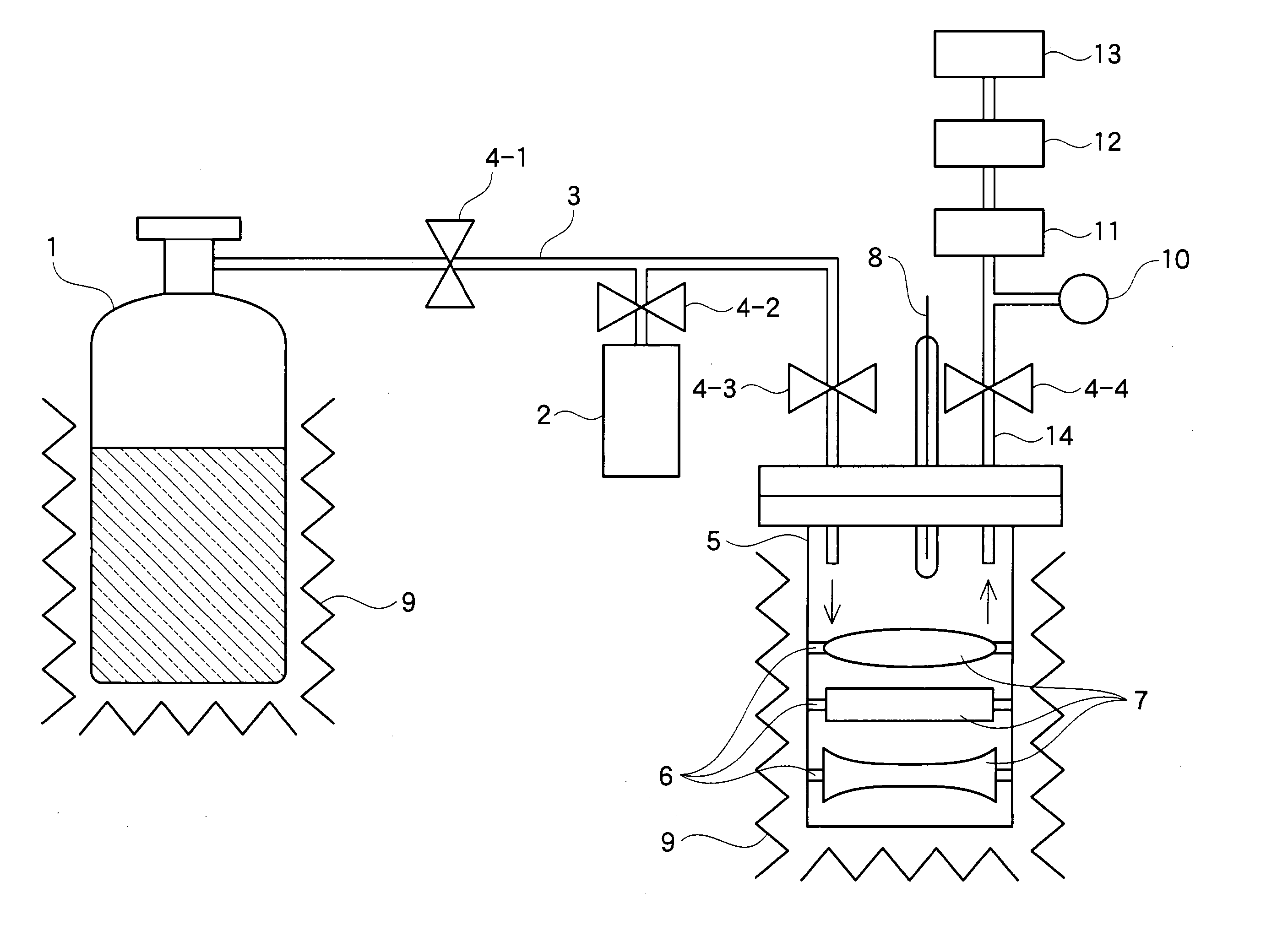
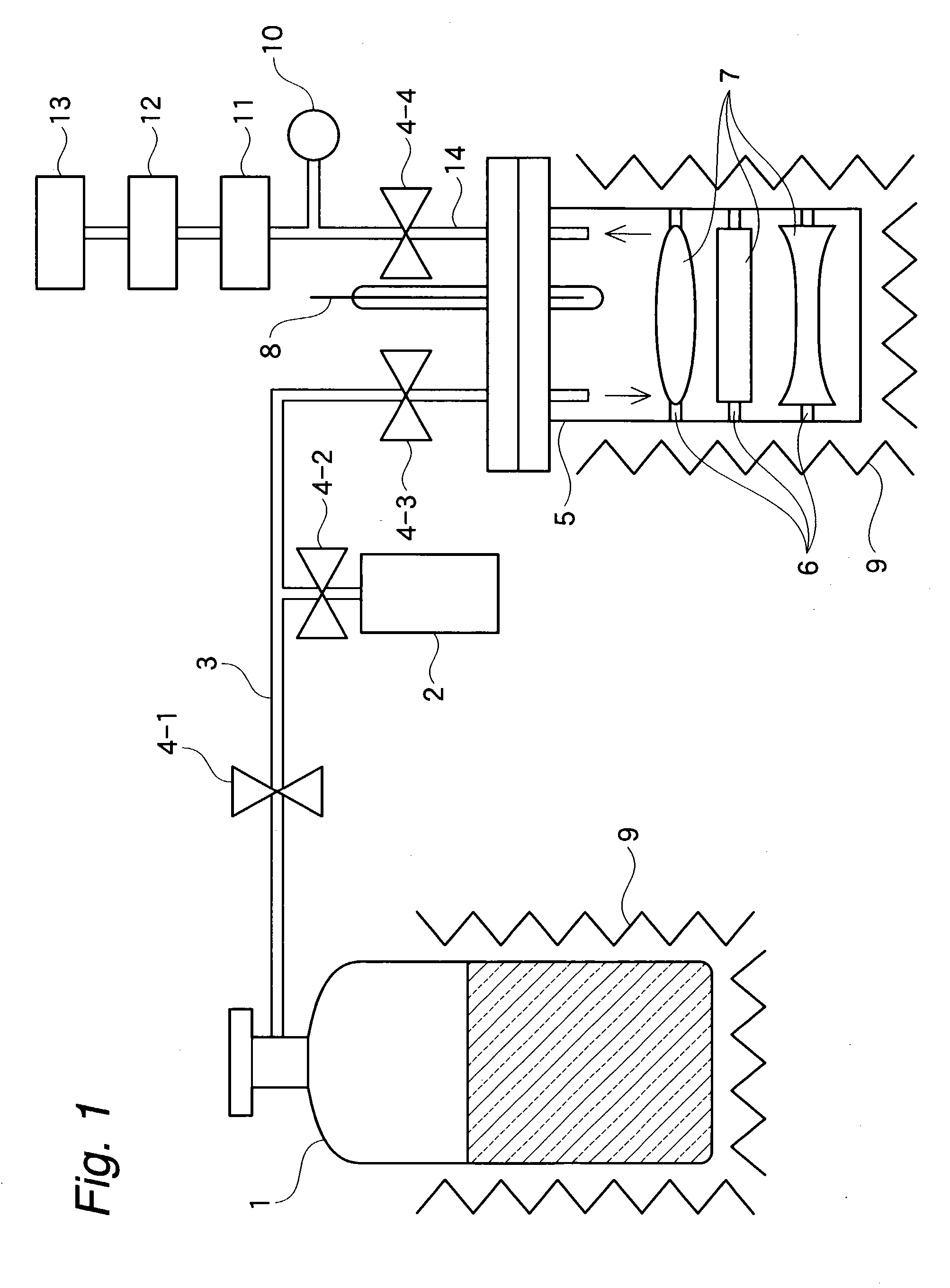
[0244] In this example 1, a fluorination apparatus having a structure as shown in FIG. 1 was used and in a gas pipe 3 and an exhaust pipe 14, as shown in FIG. 1, a monel metal alloy of a nickel-copper alloy was used for a material of a section from a reactor 5 to a valve 4-4. Stainless steel valves 4-1, 4-2, 4-3 and 4-4 were dismantled and gas-contacting portions of the valves were subjected to nickel-plating so that chromium and fluorine were not contacted. By the nickel-plating, the whole fluorine gas feeding system and reaction system were completely chromium free. Samples prepared by film forming each of MgF.sub.2 and LaF.sub.3 single layer films in a film thickness of 150 nm onto a fluorite substrate were used. In a fluorination reaction step at 100.degree. C., 100% fluorine gas was fed. That is, dilution with helium was not conducted. In a subsequent heating step at 300.degree. C., fluorine gas containing 10 ppm of fluorine prepared by diluting with helium gas was introduced. ...

example 2

[0258] Utilizing the completely chromium-free experimental facility prepared in Example 1, a F.sub.2 lithography antireflection film was fluorinated. With regard to an optical element prepared by forming the antireflection films comprising MgF.sub.2 and LaF.sub.3 alternate layers on the both surfaces of a parallel and plat fluorite substrate having a thickness of 3 mm, the results of measuring a spectral transmittance are shown in FIG. 5. It was easily found that the transmittance in the vacuum ultraviolet region of a wavelength of less than 185 nm was really improved by conducting the fluorination with heat according to the present invention. With shortening the wavelength, a marked difference between the conducting of the fluorination with heat or not was recognized. The difference of the transmittance in the wavelength of 157 nm was 4%. Only one optical element had a 4% transmittance difference. Therefore, when all of the optical elements of a semiconductor exposure apparatus com...

example 3

[0260] Single crystal fluorite of calcium fluoride (CaF.sub.2) was processed to be in a parallel flat shape. The surface precise polishing (final polishing) of the single crystal fluorite was carried out by buff polishing with suede cloth dusted with a suspension prepared by dispersing silicon dioxide (SiO.sub.2) polishing abrasive grain in water to prepare a fluorite optical element having a polished surface. The resulting fluorite optical element was sucesssively washed with a neutral detergent, distilled water and isopropyl alcohol in a conventional method and thereby polishing abrasive grain and organic matters remained on the surface of the fluorite optical element were removed.

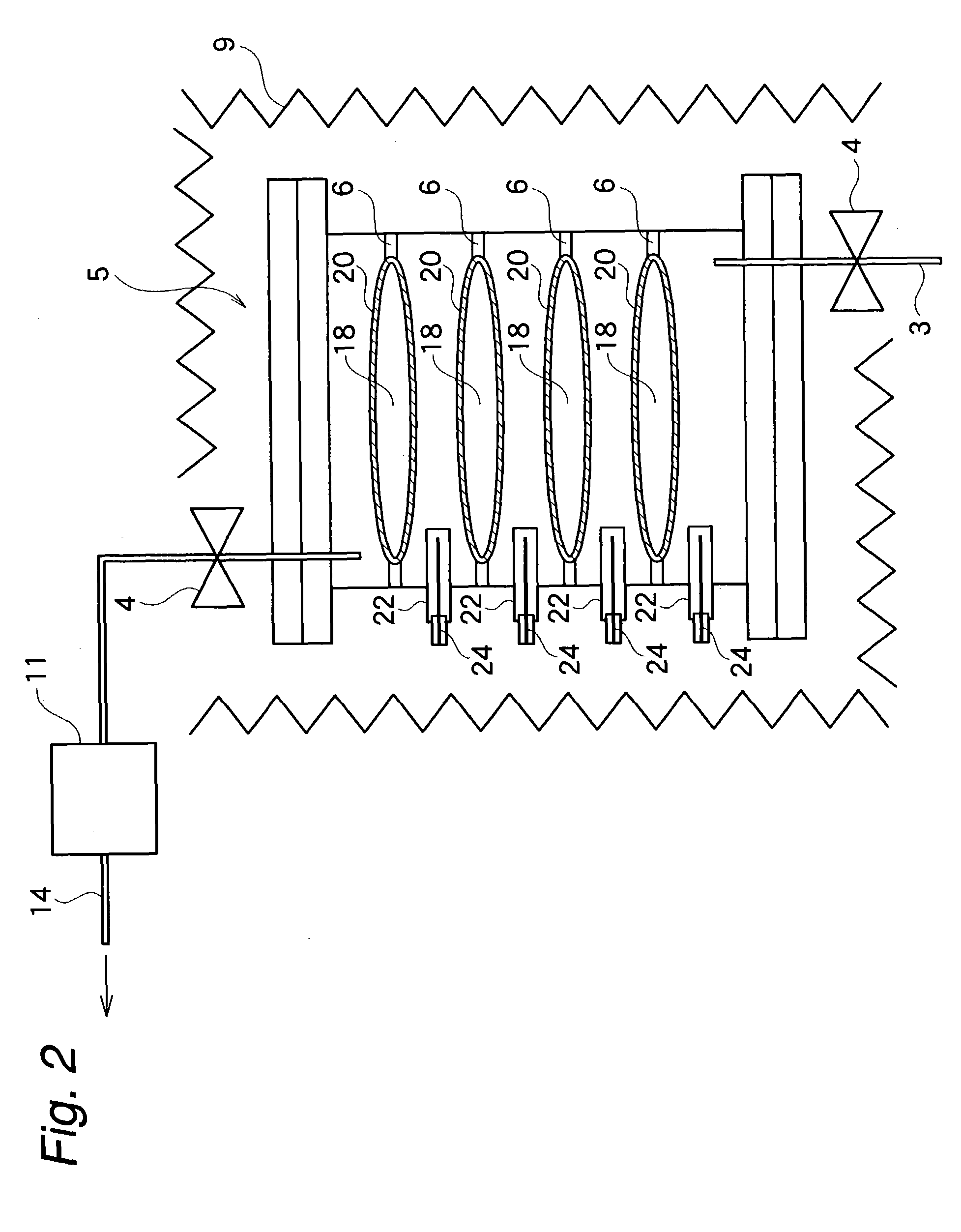
[0261] Subsequently, using a fluorination apparatus (washing apparatus) as shown in FIG. 1, the fluorite optical element was fixed to a fluoride optical element-fixing jig 6 made of pure nickel provided inside a reactor (cleaning vessel) 5 made of pure nickel and thereafter the cleaning vessel 5 was seal...


PUM

PropertyMeasurementUnit
temperatureaaaaaaaaaa
total pressureaaaaaaaaaa

Abstract

According to the invention, a fluorination treated substance remarkably reduced in the light absorption loss of a substance to be treated, such as a fluoride thin film, a fluorination treatment apparatus capable of producing the fluorination treated substance, and a process for producing a fluorination treated substance can be provided. Disclosed is a process for producing a fluorination treated substance, comprising an enclosure step of enclosing a substance to be treated in a reactor and a fluorination reaction step of introducing a fluorine gas into the reactor to bring the substance to be treated into contact with the fluorine gas and thereby carry out fluorination reaction.

Description

[0001] Priority is claimed to Japanese Patent Application No. 2002-198165, filed on Jul. 8, 2002, Japanese Patent Application No. 2003-120304, filed on Apr. 24, 2003, Japanese Patent Application No. 2003-144825, filed on May 22, 2003, U.S. Provisional Patent Application No. 60 / 397,610 filed on Jul. 23, 2002, No. 60 / 470,900 filed on May 16, 2003 and No. 60 / 473,890 filed on May 29, 2003, the disclosure of which are incorporated by reference in their entireties.[0002] This application is an application filed under 35 U.S.C. .sctn.111(a) claiming benefit pursuant to 35 U.S.C. .sctn.119(e) of the filing dates of Provisional Application No. 60 / 397,610 filed on Jul. 23, 2002, No. 60 / 470,900 filed on May 16, 2003 and No. 60 / 473,890 filed on May 29, 2003 pursuant to 35 U.S.C. .sctn.111(b).[0003] The present invention relates to a fluorination treatment apparatus for forming a fluorine atmosphere freed of impurity contamination to treat a substance to be treated, a process for producing a flu...

Claims


Application Information

Patent Timeline
Patent Type & Authority Applications(United States)
IPC IPC(8): C23C8/02C23C8/06
CPCC23C8/06C23C8/02
Inventor HOSHINO, YASUYUKITAKI, YUSUKE
Owner SHOWA DENKO KK
Why Eureka
Try Eureka