

Method of manufacturing a spectral filter for green and longer wavelengths
a technology of spectral filter and green wavelength, applied in the field of manufacturing optical filter, can solve the problems of high reflection loss caused by high refractive index, approach can also have significant disadvantages, and the level of losses of semiconductor-based long-pass filters is high, so as to reduce waveguide cross section, reduce the loss level, and increase the pore cross section
- Summary
- Abstract
- Description
- Claims
- Application Information
AI Technical Summary
Benefits of technology
Problems solved by technology
Method used
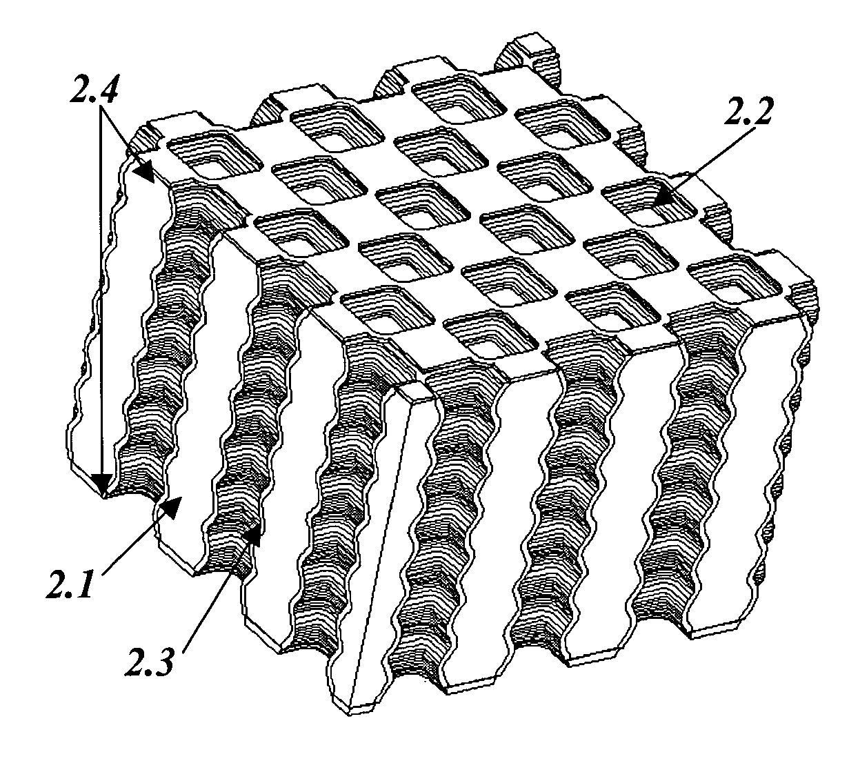
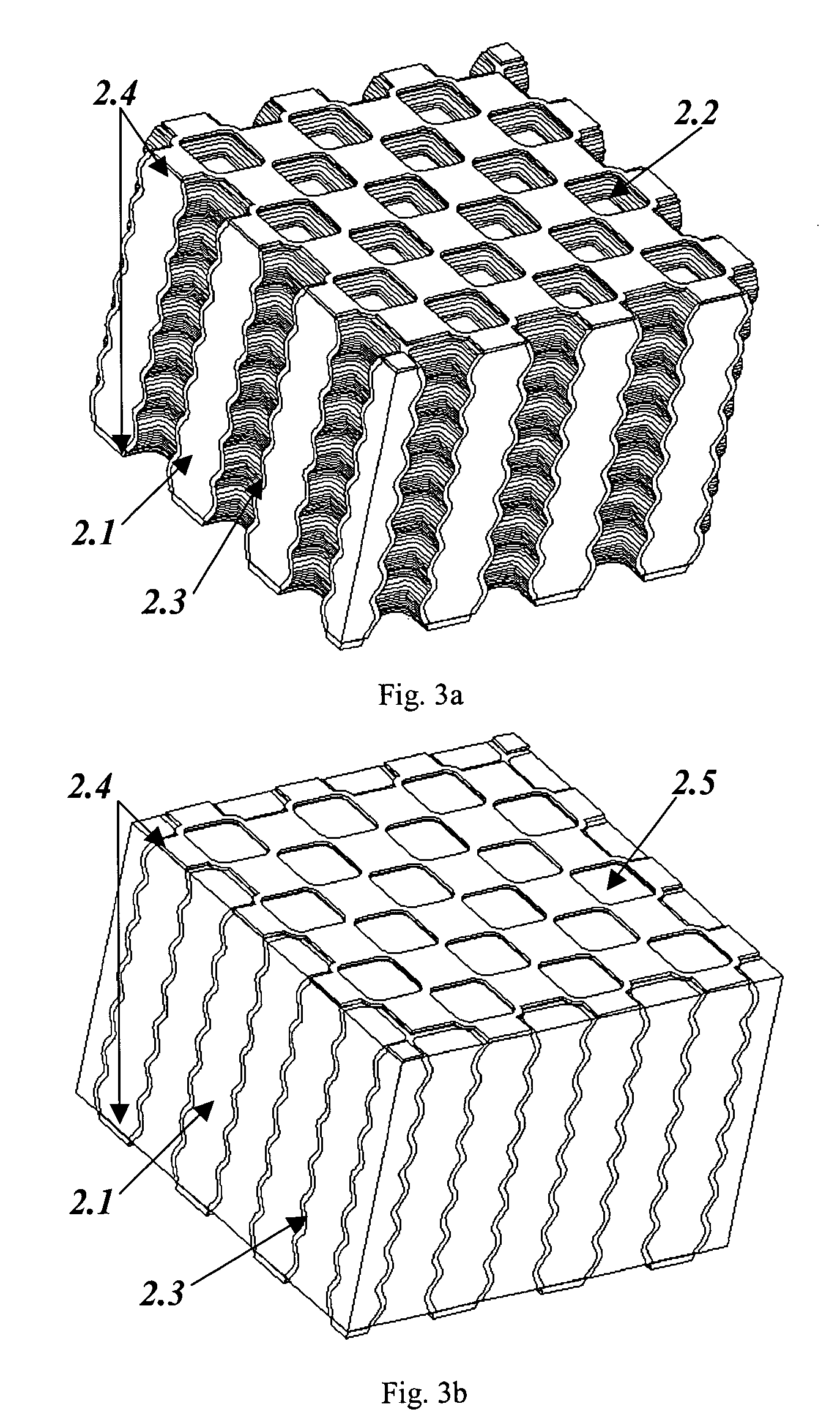
Image

Examples
example 2
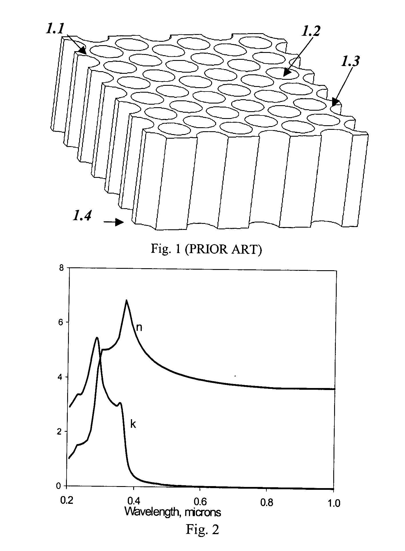
[0173] The method in Example 1 was repeated but improved by increasing the smoothness of the pore walls (reducing the optical scattering). To suppress the roughness, an SiO2 layer was grown on all surfaces of the wafer by means of thermal oxidation at 1050.degree. C. in a hot furnace in air for 2 hours. The SiO.sub.2 layer was then etched off the pore walls in HF (5 minutes in 48% aqueous solution under manual agitation). The wafer was then cleaned in deionized water for 5 minutes. A functional far IR band-blocking filter consisting of an attached MPSi layer having smoothed pore walls and thus less optical scattering was thus formed.
example 3
[0174] The method in Example 1 was repeated but modified by removing the backside of the wafer. The anodically etched wafer with closed pores was slowly inserted into a hot (1000.degree. C.) oxidation furnace tube for 4 hours to form an oxide layer on all surfaces. Then the wafer was placed into a Reactive Ion Etching machine and an opening in the oxide layer from the back side (circular, 1 inch in diameter) was formed by etching through a photoresist mask. The wafer then was waxed by its first surface to a glass 2.times.2 inch wafer and placed into a hot KOH solution (the same as during etch pit process) for 12 hours. By this means, the non-porous part of the silicon wafer was removed. The wafer was then placed into an acetone bath for 6 hours to strip it from the glass plate and to remove the wax. A functional far IR band-blocking filter consisting of a free-standing MPSi layer was thus formed.
example 4
[0175] In a fourth example, a p-doped, double-side polished (100) higher-resistivity Si wafer and a different electrolyte were used. The resistivity was in the 67.9-73 Ohm*cm range as measured by the vendor. The wafer was oxidized in a hot tube furnace in air (1000.degree. C.) for 4 hours, producing 200 nm of oxide on all surfaces of the silicon. The wafer was photolithographically patterned from the first side of the wafer (i.e. holes in a photoresist layer were formed at the predetermined locations). The pattern was of cubic symmetry with round holes spaced 5 .mu.m apart and having diameters of 2.5 .mu.m. The photoresist pattern was transferred into the SiO.sub.2 layer through a reactive ion etching process. The subsequent etch pit formation and anodization steps were the same as in Example 1, except that the electrolyte was chosen to have the composition 25[HF]+70 [Ethanol]+160 [MeCN] by volume. A functional far IR band-blocking filter was thus formed.
PUM
| Property | Measurement | Unit |
|---|---|---|
| Thickness | aaaaa | aaaaa |
| Thickness | aaaaa | aaaaa |
| Fraction | aaaaa | aaaaa |
Abstract
Description
Claims
Application Information