Monolithic light emitting devices based on wide bandgap semiconductor nanostructures and methods for making same

a nanostructure, monolithic technology, applied in the field of nanolithography, can solve the problems of low quality, low cost effective and low-defect materials, and high density of threading dislocation, and achieve the effects of low cost, reduced defects, and high degree of size control and/or uniformity

Inactive Publication Date: 2005-04-21
GENERAL ELECTRIC CO
View PDF1 Cites 146 Cited by
  • Summary
  • Abstract
  • Description
  • Claims
  • Application Information

AI Technical Summary

Benefits of technology

[0014] The present invention provides a simple, monolithic white LED device based on quantum confined, low-defect wide bandgap nanostructures of varying size. Reduction in defects and greater control over size significantly increases the tunability and emission efficiency of the LED.
[0015] By providing greater control over size uniformity, the present invention also provides a practical method for uniformly generating monodisperse quantum dots which can be used in quantum dot laser diodes (QDLDs) to produce monochromatic light.
[0016] The present invention provides a method of using nanolithographic techniques and exploiting quantum confinement and surface elasticity effects to intelligently nanostructure materials for use as efficient, monolithic white LEDs. Control over the types of materials, size effects, and surface effects permits the tuning of emission wavelengths by a number of different parameters, and the combination of quantum confinement and surface elasticity effects permits the tuning of the emission on larger size scales, making fabrication easier and less expensive.

Problems solved by technology

A key challenge, and also a main research focus in the development and application of wide band gap technology, particularly gallium nitride (GaN), is the lack of high quality, cost effective and low-defect materials.
Due to a lack of a commercially available low-defect GaN substrate material, GaN is commonly grown on substrates such as sapphire, silicon carbide, zinc oxide, silicon, etc.
High densities of threading dislocation ensue due to lattice and thermal mismatches with these substrates.
Lateral epitaxial overgrowth, pendeo-epitaxy, and bulk homo-epitaxial growth techniques have been proposed to improve the quality of GaN material, yet none of these techniques are currently optimal.
The problems associated with this approach are low emission efficiency, Stokes losses, device lifetime, and complex packaging (because a phosphor layer must be manufactured into the device).
This approach is very expensive and complex since each of the blue, green and red LEDs have to be addressed independently and a feedback mechanism is needed.
However, current attempts to capitalize on QDs for lasing applications are limited by the inability to form uniform, monodisperse dots throughout a film.
Control over the uniformity (both size and composition) of these nanostructures in the active layer of the LED devices remains a major challenge, however.
The device itself was based on multiple quantum wells, and the internal quantum efficiencies were severely limited by size disorder and spatial non-uniformity.
Defect reduction through strain relief inside 3-dimensional (3-D) confined nanostructures grown on lattice-mismatched substrates has not yet been attempted based upon a systematic size and shape optimization via physical modeling of the phenomena of dislocation nucleation.
However, this technique does not generate low-defect GaN because the sputtered structures cannot be controllably ordered and made monodisperse.
Further, the techniques used to generate the nano-columns rely on sputtering conditions and not nanolithography patterning.
However, Lieber et al. have only succeeded in making monochromatic (single wavelength) LEDs.
To date, however, block co-polymers (or other lithographic techniques) have not been used for the templated growth of quantum dots (or other nanostructures) that present a large lattice mismatch with the corresponding substrate.

Method used


Image

  • Monolithic light emitting devices based on wide bandgap semiconductor nanostructures and methods for making same
  • Monolithic light emitting devices based on wide bandgap semiconductor nanostructures and methods for making same
  • Monolithic light emitting devices based on wide bandgap semiconductor nanostructures and methods for making same

Examples


example 1

[0075] This example serves to illustrate the role modeling plays in determining optimum material selection for the wide bandgap material nanostructures and the substrate / nucleation layer.

[0076] A three-dimensional model has been developed to help predict and optimize the nano-template chemical composition, geometry, and dimensions for which low-defect wide band gap nanostructures are obtained. The models for misfit dislocation nucleation are formulated with the aid of numerical finite element simulations and approximate dislocation energetics, and are an extension of the Jain and Atkinson models for 2-dimensional stripes into 3-dimensions (Atkinson et al., J. Appl. Phys., 72, p. 2242, 1992); Jain et al., J. Appl. Phys., 78, p. 1630, 1995; Atkinson et al., J. Appl. Phys., 77, p. 1907, 1995). One of the outputs of the model is a dislocation density map for various nano-island chemical composition, shape, and dimension combinations. In particular, critical combinations (i.e., cylinder...

example 2

[0078] This example serves to illustrate the nanolithographic process using block co-polymer lithography as an exemplary nanolithographic means.

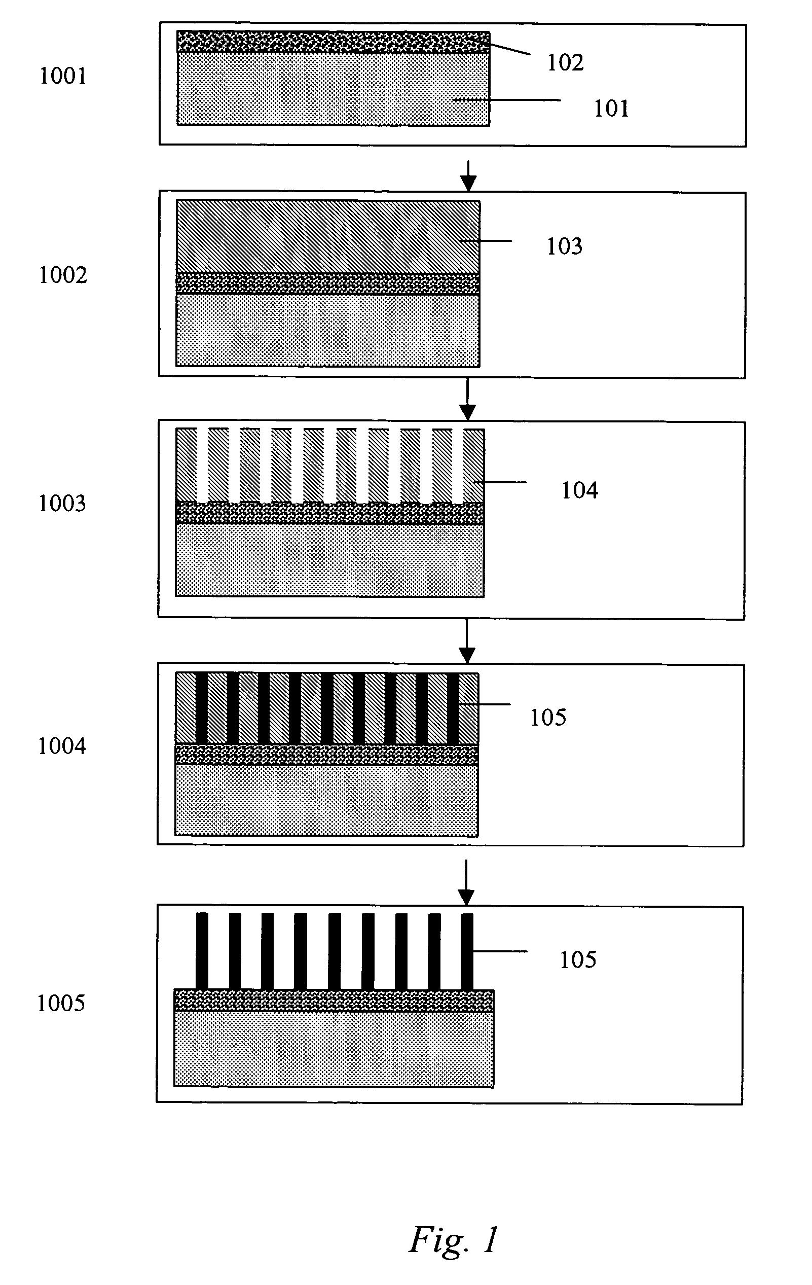
[0079] Referring to FIG. 6, a self-assembled block co-polymer thin film 601 (e.g., PS-PMMA) is deposited on top of the sacrificial dielectric layer 103 in step 6001. Selective removal of one of the block co-polymer phases with chemical and / or radiation treatments yields a nano-lithographic mask composed of a nano-porous polymeric film 602, as shown in step 6002. In step 6003, chemical treatment and / or reactive ion etching (RIE) and pattern transfer to the sacrificial layer yields the nano-porous template or mold 104 in which wide bandgap material nanostructures 105 can be grown as in step 6004. FIG. 7 depicts a scanning electron micrograph of a surface that has been patterned using block co-polymer lithography.

example 3

[0080] This example serves to illustrate the effect of surface elasticity on the emission properties of “embedded” wide bandgap nanostructures.

[0081] As mentioned in the background section, at the nanoscale, size-related quantum confinement effects have a large influence on the emission wavelength of light. Applicant has recently demonstrated that surface elasticity (nano-strain) effects at the nanoscale level can also cause a dramatic shift in the emission wavelength of embedded quantum dot nanostructures (Sharma et al., Phys. Stat. Sol. B, 234(3), R10-R12 (2002); Sharma et al., “Effects of Surface Elasticity in Nano-Inhomogeneities, Nanocomposites, and Quantum Dots,” ASME Mechanics of Materials Conference, Scottsdale, Ariz. (2003); both of which are incorporated herein by reference). Hydrostatic strain state within a QD structure is known to impact that structure's optoelectronic properties. Several works, of varying sophistication (both analytical and numerical), have focused on...


PUM

PropertyMeasurementUnit
thicknessaaaaaaaaaa
pore radiiaaaaaaaaaa

Abstract

The present invention is directed toward a method for fabricating low-defect nanostructures of wide bandgap materials and to optoelectronic devices, such as light emitting sources and lasers, based on them. The invention utilizes nanolithographically-defined templates to form nanostructures of wide bandgap materials that are energetically unfavorable for dislocation formation. In particular, this invention provides a method for the fabrication of phosphor-less monolithic white light emitting diodes and laser diodes that can be used for general illumination and other applications.

Description

TECHNICAL FIELD [0001] The present invention relates generally to electroluminescent light sources, and more specifically to the use of nanolithography to enable the generation of low-defect nanostructures and to tailor the emission of such light sources to a particular wavelength or range of wavelengths by exploiting quantum confinement and surface elasticity effects. BACKGROUND INFORMATION [0002] A key challenge, and also a main research focus in the development and application of wide band gap technology, particularly gallium nitride (GaN), is the lack of high quality, cost effective and low-defect materials. Due to a lack of a commercially available low-defect GaN substrate material, GaN is commonly grown on substrates such as sapphire, silicon carbide, zinc oxide, silicon, etc. High densities of threading dislocation ensue due to lattice and thermal mismatches with these substrates. Lateral epitaxial overgrowth, pendeo-epitaxy, and bulk homo-epitaxial growth techniques have bee...

Claims


Application Information

Patent Timeline
Patent Type & Authority Applications(United States)
IPC IPC(8): G02B6/122H01L27/15H01L33/24H01S5/183H01S5/34
CPCB82Y20/00G02B6/1225H01L33/24H01S5/423H01S5/183H01S5/3412H01S5/1042
Inventor ALIZADEH, AZARSHARMA, PRADEEPLEBOEUF, STEVEN FRANCISGANTI, SURYAPRAKASHD'EVELYN, MARK PHILIPCONWAY, KENNETH ROGERSANDVIK, PETER MICAHTSAKALAKOS, LOUCAS
Owner GENERAL ELECTRIC CO
Why Eureka
Try Eureka