[0007] According to one feature of this invention, an
optical communication system comprises at least one monolithic
semiconductor photonic
integrated circuit chip having a plurality of communication signal channels formed on the chip, each of the signal channels including at least one active optical component optically coupled with a means to either optically combine or decombine channel signals on the
semiconductor chip. A booster
optical amplifier is optically coupled to a port on the chip to amplify channel signals to be received into or transmitted out of the chip. The booster optical
amplifier can be a low performance
fiber amplifier, such as, for example, an EDFA, or a semiconductor optical
amplifier (SOA), semiconductor
laser amplifier, a
gain-clamped-SOA or concatenated amplifiers of any of the foregoing types of semiconductor optical amplifiers. One particular example of a PIC chip utilizing such a booster optical amplifier is a semiconductor monolithic
transmitter photonic
integrated circuit (TxPIC) chip. The booster optical amplifier is used instead of deploying semiconductor optical amplifiers directly integrated on the TxPIC chip to provide required
gain for generated on-chip channel signals. By eliminating these integrated
gain components fro the PIC chip, the complexity of the PIC chip can be reduced, which translates into less on-chip contacts and less applied current and bias necessary to the chip and, correspondingly, lower on-chip
heat generation that must be dissipated.
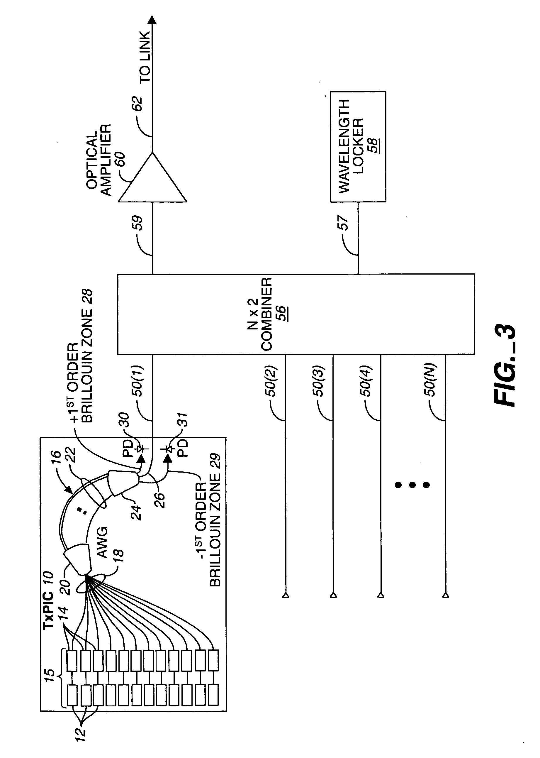
[0008] A further feature of this invention is the method of deploying a passive optical combiner that is a
broad bandwidth spectral
wavelength combiner for combining the outputs from multiples transmitter photonic
integrated circuit (TxPIC) chips and, thereafter, the amplification of the combined channel signals with a booster optical amplifier couple between the passive optical combiner and the
fiber transmission link. The booster optical amplifier may be a rear earth
fiber amplifier, such as an
erbium doped
fiber amplifier (EDFA), or one or more semiconductor optical amplifiers (SOAs) on one or more semiconductor chips. Such a combination of optical components simplifies the design of individual TxPICs and other such
optical communication PICs, which has to take into consideration the nonlinear effects of difficult, high loss single mode fiber (SMF) links or other fiber-type links by allowing a
higher power per channel to be achieved compared to the case where channel amplification is attempted directly on the TxPIC chip through the deployment of on-chip optical amplifiers, such as semiconductor optical amplifiers (SOAs), integrated in locations following the electro-optic (EO) modulators, if not integrated also at other locations on the same chip.
[0009] By removing the channel
signal amplification requirement from the TxPIC chip, the TxPIC design and the amplification required components is simplified in several ways. First, the on-chip active optical components is reduced to the arrays of lasers sources and EO modulators (and possibly at least one array of photodetectors) as well as the passive optical combiner, thereby lowering on-chip
power consumption by as much as 40% and, correspondingly, the amount of on-chip heat generated that must be carried away off-chip. Second, the number of required on-chip contacts is reduced. Third, the possible optical and / or thermal interactions of on-chip optical amplifiers with other on-chip active optical components, such the
laser sources and the EO modulators, are eliminated. Fourth, two-
photon absorption (TPA) possibly occurring in the optical combiner is significantly reduced if not eliminated. Fifth, the launch power per channel is set by the booster optical amplifier rather than via any on-chip semiconductor amplifiers so that the total launch power for all channels can be adjusted to meet the different loss requirements of different high loss, single mode fiber (SMF) optical spans or links. Sixth, on-chip SOAs in each channel path can degrade the
extinction ratio of the EO modulators. As a result, operation of the SOAs would have to be sufficiently backed off of saturation to prevent such degradation, which may be several dB, which defeats, in part, the purpose of providing on-chip amplifiers. Seventh, with no on-chip semiconductor optical amplifiers, any negative
impact of ASE
noise feedback from such on-chip amplifiers back into on-chip electro-optic modulators is eliminated. Such ASE feedback would significantly affect the
extinction ratio of the modulators.
[0010] A further
advantage of the deployment of a low cost, low performance booster optical amplifier at the output of a TxPIC
semiconductor chip is that the amplifier, such as in the case of an EDFA, need not be a high performance, expensive optical amplifier and, therefore, providing a significantly cost-effective approach for achieving desired gain per channel. In this regard, the EDFA may be a
single stage EDFA with one pump laser where the amplifier stage is only a few meters long. This compares to a high performance amplifier that has
multiple stages and two or more pump lasers and is many meters long, such as the type deployed for mid-span optical amplification.
[0011] Also, in the case of multiple PIC chip outputs combined via an optical combiner, such as a power coupler or a
star coupler, the deployment of an relatively inexpensive optical amplifier at the optical combiner output permits the use of a less expensive optical combiner, as opposed to an interleaver or
multiplexer, which couplers have no
wavelength selective
passband effect or guardbands but do experience higher optical losses. Thus, an inexpensive optical amplifier following such a
broad bandwidth spectral
wavelength combiner complements the higher
insertion loss of such a combiner with sufficient per
channel gain eliminating the need for a more expensive band interleaver or
multiplexer having
passband selective effects although providing comparatively lower optical losses.

