

Antireflective film-forming composition, method for manufacturing the same, and antireflective film and pattern formation method using the same
a technology of anti-reflective film and composition, which is applied in the direction of photosensitive materials, instruments, photomechanical equipment, etc., can solve the problems of resist pattern shape tapering, halation, and insufficient precision of achromatic lenses or aspherical reflective optical systems, and achieve high etching selection ratio, fast etching speed, and excellent pattern
- Summary
- Abstract
- Description
- Claims
- Application Information
AI Technical Summary
Benefits of technology
Problems solved by technology
Method used
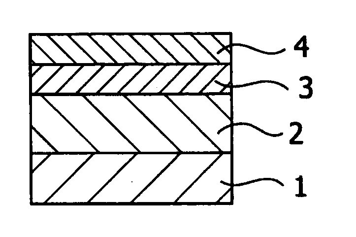
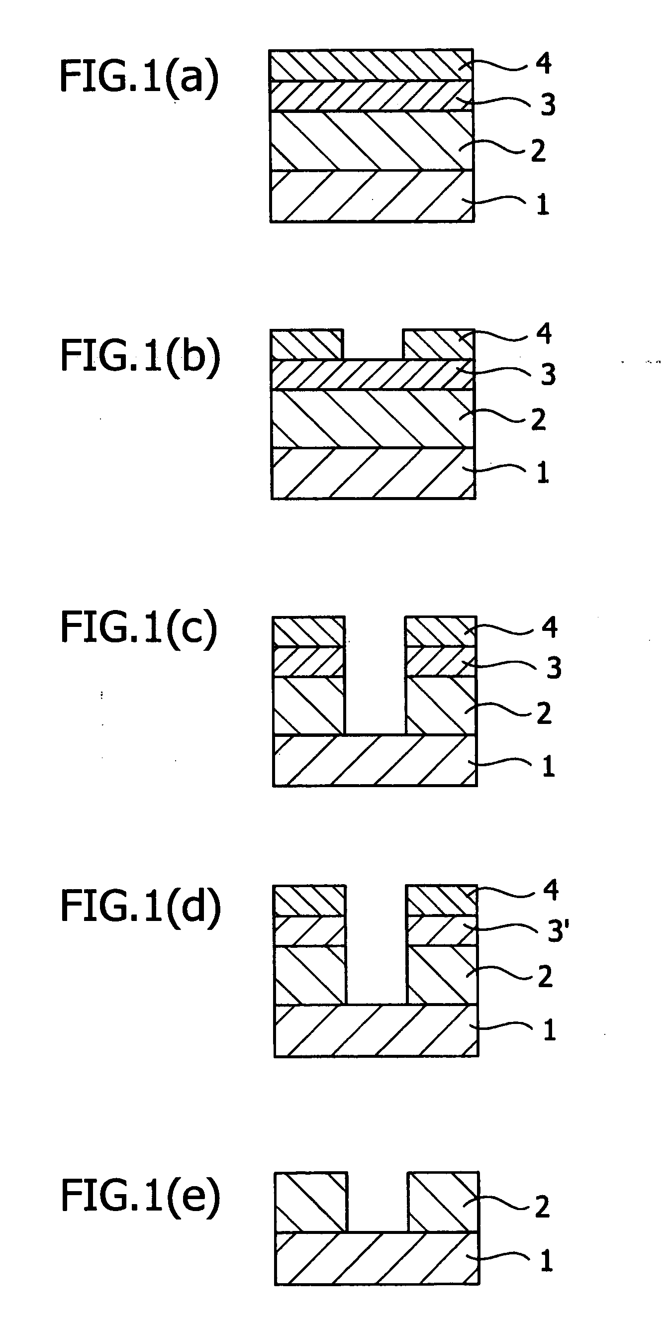
Image

Examples
working examples
[0155] Hereinafter the present invention is described in further detail through manufacturing examples, working examples and comparative examples but the present invention is not limited to the following descriptions.
manufacturing example 1
[0156] 252 g of ultrapure water, 770 g of ethanol and 440 g of 10% tetramethylammonium hydroxide solution were prepared in a 3 L flask, to which a fluid mixture of 27 g of 3-acetoxypropyltrimethoxysilane, 14 g of phenyltrimethoxysilane and 51 g of 3-(2′-methoxypropoxy) propyltrimethoxysilane was added, and mixed well in a nitrogen atmosphere at 30° C. After one hour, 35 g of acetic acid was added, and the ethanol and methanol were removed by distillation at reduced pressure (100 hPa) 900 g of ethyl acetate was added to the remaining liquid, and after separating the water phase, the organic phase was washed 5 times with 300 g of ultrapure water. Into the organic phase 200 g of propylene glycol monomethyl ether acetate was added, concentrated under reduced pressure (20 hPa), yielding 250 g of a solution of a polymer 1. The non-volatile matter was 16 wt %.
manufacturing example 2
[0157] 84 g of ultrapure water, 256 g of ethanol and 29 g of 10% tetramethylammonium hydroxide solution were prepared in a 1 L flask, to which a fluid mixture of 7.5 g of 2-acetoxymethyl-bicyclo[2.2.1]heptanyltrimethoxysilane, 6.3 g of phenyltrimethoxysilane and 22.4 g of 3-(2′-methoxypropoxy) propyltrimethoxysilane was added, and mixed well in a nitrogen atmosphere at 30° C. After one hour, 1.6 g of acetic acid was added, and the ethanol and methanol were removed by distillation at reduced pressure (100 hPa). 300 g of ethyl acetate was added to the remaining liquid, and after separating the water phase, the organic phase was washed 5 times with 70 g of ultrapure water. Into the organic phase 100 g of propylene glycol monomethyl ether acetate was added, concentrated under reduced pressure (20 hPa), yielding 85 g of a solution of a polymer 2. The non-volatile matter was 28 wt %.
PUM
| Property | Measurement | Unit |
|---|---|---|
| temperature | aaaaa | aaaaa |
| refractive index | aaaaa | aaaaa |
| refractive index | aaaaa | aaaaa |
Abstract
Description
Claims
Application Information