Surface-coating method, production of microelectronic interconnections using said method and integrated circuits

a microelectronic and surface coating technology, applied in the direction of coatings, electrical equipment, liquid/solution decomposition chemical coatings, etc., can solve the problems of increasing the pressing of etching and the inability to apply certain processes and devices described below for microelectronics in these fields, and the resistance is increasingly unacceptabl

Inactive Publication Date: 2006-09-21
COMMISSARIAT A LENERGIE ATOMIQUE ET AUX ENERGIES ALTERNATIVES +1
View PDF12 Cites 72 Cited by
  • Summary
  • Abstract
  • Description
  • Claims
  • Application Information

AI Technical Summary

Benefits of technology

[0062] Proceeding in this manner avoids having to reprovision with metallization precursors from the solution, especially in the most conducting regions, if they exist, and overcomes any electroplating or electroless plating irregularities in this step of producing the seed layer—the construction of the metal film (by reduction) is promoted at the place where the precursors have been trapped, thanks to the organic film, and only at this point, that is to say on or in a uniform ultrathin film conformal with the surface structure of the barrier layer.
[0063] When the film is covered and/or filled with the precursors of the metallic material on leaving the first bath, the concentration gradients between the film (filled with precursors) and the solution of the second bath (containing no precursor...

Problems solved by technology

In what follows, the prior art is restricted to the microelectronics field as this is representative of both devices and processes currently available for uniform metal deposition and of the increasing technical difficulties in obtaining uniform—and especially conformal—metal coatings as the demand for faster processors and ever finer etching becomes more pressing.
A person skilled in the art may therefore easily transpose these problems to other applications, such as microsystems or connectors, the problem being the same at a simply different scale.
At the very most, new constraints, especially cost constraints, are appearing that mean that certain processes and devices described below for microelectronics cannot be applied in these fields.
When these interconnects are made of aluminium or tungsten, they therefore result in increasingly unacceptable resistances as their size decreases.
This is because such high resistances increase the impedance of the circuits, increase the electrical signal propagation times and they limit the clock speeds of micro-processors.
In addition, at high current densities aluminium is liable to undergo electromigration.
This may occur in conductors of very small cross section and may cause discontinuities, leading to circuit malfunctions.
Unfortunately, the techniques currently available for fabricating interconnects, particularly copper interconnects, are not sufficiently precise for interconnects below 100 nm and/or incur very high costs.
Although copper is used most in current techniques, the alternative of copper interconnects is faced with two major problems, namely copper is difficult to etch (it is therefore not possible to produce, in a simple fashion, the wiring patterns by processes of this type, albeit conventional processes); and copper is an element with a high rate of diffusion into many materials.
This diffusion may lead to the short-circuiting of neighbouring tracks, and therefore to overall malfunction of the circuit.
Now, this distribution is typically very non-uniform in the case of an extended semiconducting surface, like that offered by the barrier layer deposited over the entire substrate wafer used for fabricating the integrated circuit.
Since the materials used for the barrier layer (titanium nitride, tantalum nitride, tungsten carbide, etc.) are semiconductors, their conductivity is insufficient to allow uniform copper deposition.
The three steps require the use of two pieces of equipment, one for the PVD/CVD and the other for the electroplating or for the autocatalytic (electroless) step, which incurs a high cost for implementing these techniques.
However, it is observed that copper coatings deposited by PVD exhibit low step coverage when the aspect ratios are high (that is to say the number of recesses and/or etched features is high), which is the case in the production of interconnect lines and vias.
However, for most precursors, copper deposited by CVD exhibits poor adhesio...

Method used


Image

  • Surface-coating method, production of microelectronic interconnections using said method and integrated circuits
  • Surface-coating method, production of microelectronic interconnections using said method and integrated circuits
  • Surface-coating method, production of microelectronic interconnections using said method and integrated circuits

Examples


example 1

Filling of an Ultrathin Film of poly-4-vinylpyridine (P4VP) Electrografted onto Gold with Ionic Precursors

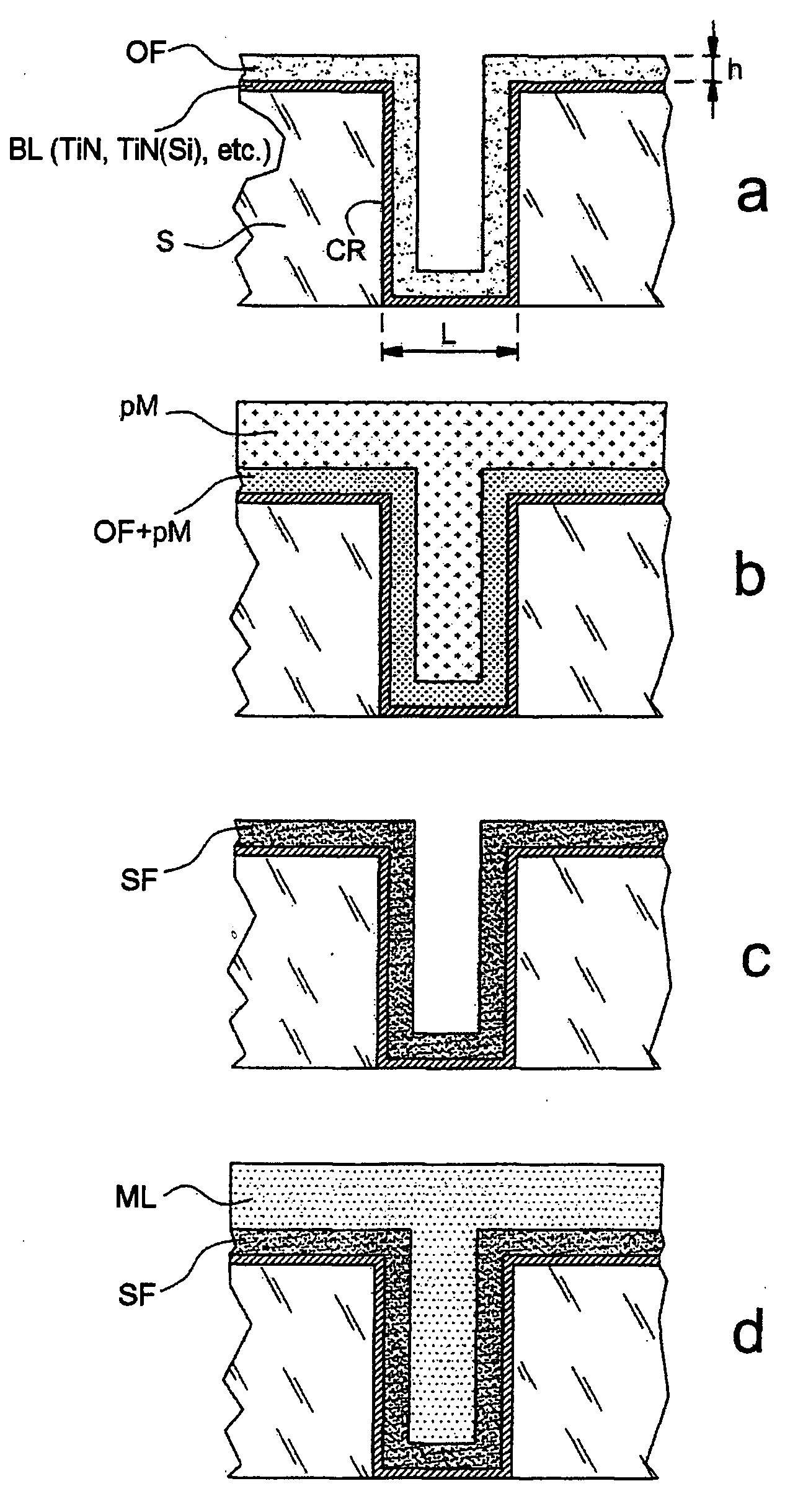
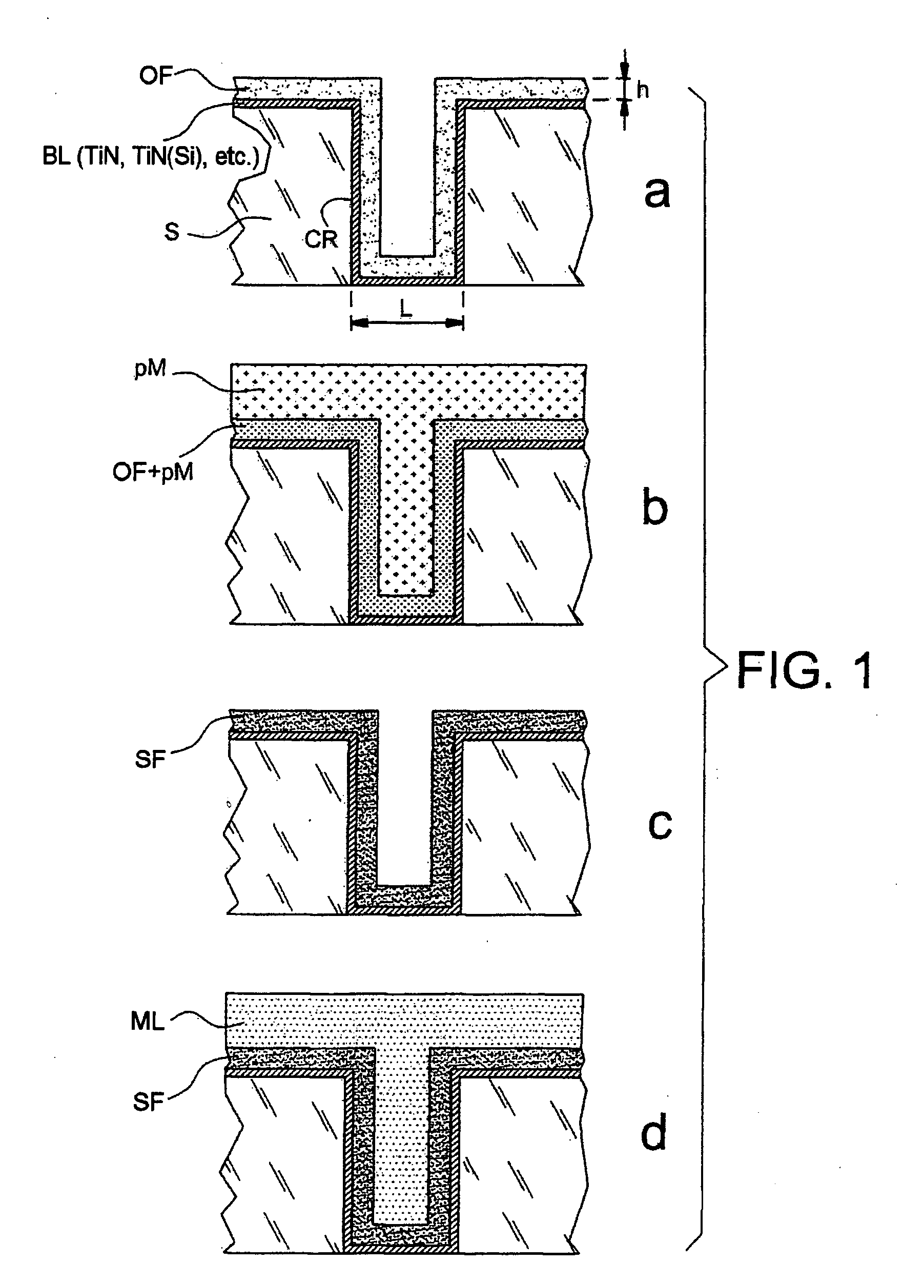
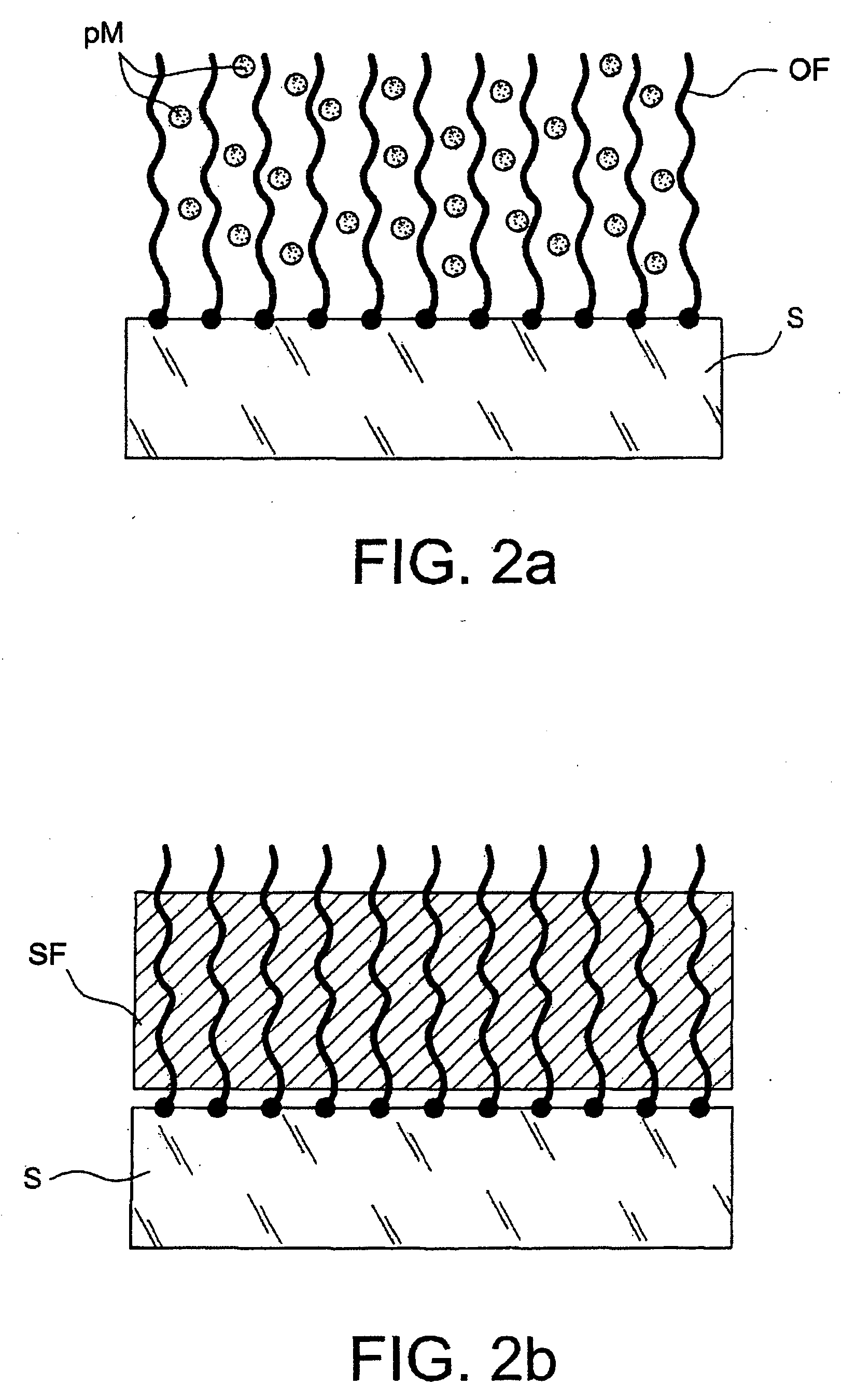
[0134] This example demonstrates that the present invention makes it possible to retain, and make use of, the complexation properties of a poly-4-vinylpyridine (P4VP) film, even when this is very thin—in this case it may have a thickness of around 30 nm.

[0135] This example illustrates, generically, the fact that an ultrathin organic film can be filled with metal precursors in ionic form. It also illustrates the fact that the complexing properties of the film are a good means of overcoming the spontaneous re-expulsion of the precursors out of the film when this film, once it has been filled and despite the unfavourable diffusion gradients, is dipped into a solution containing no precursors.

[0136] Starting with a gold strip—5 μm of gold evaporated by Joule heating onto a glass microscope slide, pretreated with a film of chromium serving as adhesion primer—an electrografted P4VP...

example 2

Electroreduction of Metal Precursors within an Ultrathin Film of poly-4-vinylpyridine (P4VP) Electrografted onto 316L Stainless Steel

[0141] This example illustrates the reduction of precursor ions trapped beforehand in a polymer film electrografted onto a metal surface. A metal film, identifiable by photoelectron spectroscopy, was thus able to be formed within the electrografted film. The reduction was carried out by electrolysis in a solution containing precursor ions. This also illustrates the fact that it is possible to obtain a metal film within an organic film according to one method of implementation in which the trapping of the precursors and the formation of the metal film take place in a single bath.

[0142] A thin P4VP film was formed using the same protocol as that of the above Example 1 on three 316L stainless steel strips (strips (a), (b) and (c)) measuring 1×10 cm, degreased beforehand by ultrasonic treatment in dichloromethane. The strips were rinsed with DMF, dried i...

example 3

Direct Attachment of a Seed Film from an Organic Film of a Polymer Deposited by Spin Coating

[0146] This example illustrates the formation of a metal film from precursors of the metallic material that are trapped in a polymer film simply deposited on a metal surface by spin coating. The polymer was resistant to the dipping bath, which allowed the precursors to be trapped owing to the fact that it was merely swollen by this bath, but not being soluble therein.

[0147] In this example, the organic film was deposited by spin coating using a solution containing 5 wt % of P4VP in DMF, so as to obtain a P4VP coating of about 100 nm on a gold strip similar to that of Example 1. The strip thus treated was dried with a hair dryer and then dipped for 25 minutes into a solution containing 10 g of copper sulphate in 200 ml of deionized water in order to insert the precursor of the metallic material. The strip was then rinsed with deionized water and then immersed in an electrolysis bath containi...


PUM

PropertyMeasurementUnit
Thicknessaaaaaaaaaa
Thicknessaaaaaaaaaa
Thicknessaaaaaaaaaa

Abstract

The present invention relates to a process for coating a surface of a substrate with a seed film of a metallic material, the said surface being an electrically conductive or semiconductive surface and having recesses and/or projections. The process comprises the following: an organic film is placed on the said surface, the said film having a thickness such that the free face of this film conformally follows the recesses and/or projections of the said electrically conductive or semiconductive surface on which it is placed; a precursor of the metallic material is inserted within the said organic film placed on the said surface at the same time as, or after, the step consisting in placing the said organic film on the said surface; and the said precursor of the metallic material inserted within the said organic film is converted into the said metallic material. This process allows integrated circuits, interconnects in microelectronics and microsystems to be fabricated.

Description

TECHNICAL FIELD [0001] The present invention relates to a process for coating a surface of a substrate with a film for nucleating a metallic material, to a process for fabricating interconnects in microelectronics, and to microelectronic interconnection elements, electronic microsystems and integrated circuits obtained by these processes. [0002] The surfaces involved in the present invention have the particular feature of being electrically conductive or semiconductive surfaces and of having recesses and / or projections, which are for example microetched features, for example interconnection holes or vias intended for the production of microelectronic systems, for example integrated circuits. [0003] The invention relates in general to a process for the uniform—and especially conformal—deposition of metal layers on electrically conductive or semiconductive surfaces, and to their applications, especially to the processes and methods for fabricating integrated circuits and more particul...

Claims


Application Information

Patent Timeline
IPC IPC(8): H01L21/4763C23C18/16C23C18/18C23C18/28H01L21/768H05K3/42
CPCC23C18/1608C23C18/1653C23C18/1893C23C18/2086H01L21/76843H01L21/7685H01L21/76867H01L21/76873H01L21/76874H05K3/422H01L21/48H05K3/18H05K3/24
Inventor BUREAU, CHRISTOPHEHAUMESSER, PAUL-HENRIMAITREJEAN, SYLVAINMOURIER, THIERRY
Owner COMMISSARIAT A LENERGIE ATOMIQUE ET AUX ENERGIES ALTERNATIVES
Why Eureka
Try Eureka