Rugged MESFET for Power Applications

a technology of power applications and mesfet, which is applied in the direction of electrical apparatus, semiconductor/solid-state device manufacturing, and semiconductor devices. it can solve the problems of inefficient and unreliable operation of power mosfets, and is virtually useless at such low-voltage, so as to reduce the risk of schottky barrier, reduce the risk of mesfet gate leakage and impact ionization, and reduce the effect of electric field

Inactive Publication Date: 2007-05-31
ADVANCED ANALOGIC TECHNOLOGIES INCORPORATED
View PDF5 Cites 26 Cited by
  • Summary
  • Abstract
  • Description
  • Claims
  • Application Information

AI Technical Summary

Benefits of technology

[0042] One aspect of the present invention provides a MESFET device with improved avalanche capability. This is accomplished by eliminating the high-field point between gate and drain along the device's etched mesa surface by enclosing the drain concentrically by both gate and source regions. In such designs, no Schottky junctions are located touching, abutting or overlapping the mesa etched surface. For a typical example, a MESFET is fabricated as a square drain region surrounded by a ring-shaped Schottky gate. The gate is surrounded, in turn by a source region so that no Schottky junction or interface is exposed to the MESFET's outer edge. The source forms the outer edge of the MESFET. Since the source is generally biased to the same potential as the package leadframe on which the die is mounted, and since no voltage differential exists between this outer die edge and its surroundings, there is no reason to perform a mesa etch. Instead the die separation through sawing is adequate to isolate devices without the need for an expensive and time consuming deep-mesa etch process common to radio frequency (RF) MESFETs.
[0044] Another aspect of the present invention provides a MESFET device that reduces MESFET gate leakage and impact ionization by eliminating the risk of the Schottky barrier touching or nearly touching the trench gate sidewall as a result of photomask misalignment. For a MESFET of this type, a trench gate is formed in a mesa of an N—GaAs epitaxial layer. The epitaxial layer is formed on top of a semi-insulating substrate. N+ regions on either side of the trench comprise the MESFET's source and drain regions. Each has its own metal contact. Schottky metal is positioned inside of the trench with another metal contact. A sidewall spacer lines the edges of the trench preventing the Schottky metal from touching the trench sidewalls. Compared to conventional MESFET structures, this sidewall spacer trench gated MESFET is unique in its low electric field, minimal leakage current along the trench sidewall, and insensitivity to photomask misalignment. It also prevents metal from ever coming in contact with the trench sidewall, eliminating the risk of unwanted metal residues on the trench sidewall.
[0045] Another aspect of the present invention provides several methods for preventing MESFET damage in avalanche. For one of these methods, a voltage clamp is used to limit the maximum drain-to-source voltage of a MESFET. The voltage clamp is implemented as a Zener diode connected in parallel with the MESFET where the breakdown of Zener diode is less than the breakdown voltage of the MESFET in its off state. The MESFET and Zener diode are preferably formed as separate die included in a single package. Fast voltage clamping may be achieved by paralleling the Zener diode and MESFET through wire bonds, thereby minimizing interdevice inductance, ringing, and voltage overshoot. To parallel the devices, the MESFET's drain electrode is connected to the Zener cathode and the MESFET's source electrode is connected to the Zener anode. The Zener clamp allows the MESFET to operate asymmetrically with respect to drain voltages, blocking current in one direction up to the Zener breakdown voltage BVZ, and conducting current through the Zener in the opposite polarity thereby limiting the maximum reverse voltage to the forward diode voltage Vf of the Zener.
[0046] In an alternative embodiment, two back-to-back series-connected Zener diodes together form a voltage clamp in parallel with the MESFET's source-to-drain terminals. The back-to-back Zener diodes may be connected in series with either a common anode or a common cathode connection, and protect the MESFET's drain-to-source terminals in either polarity operation. In a preferred embodiment each diode should have the same Zener breakdown voltage. The symmetric Zener clamp allows the MESFET to operate symmetrically with respect to drain voltages, blocking current in either direction up to the Zener breakdown voltage BVZ. In another embodiment the two Zener diodes are fabricated in a single silicon die, packaged in a single package with a power MESFET, and connected to said MESFET using bond wires.
[0048] A modification to this type of voltage clamp, adds a diode in parallel to (but oriented in the opposite polarity to) the series of forward biased diodes. This “anti-parallel” diode has no effect on the forward blocking characteristics of the diode series. In the reverse direction, the anti-parallel diode forward biases, and thereby limits the maximum reverse voltage to one VD. This voltage, while too low to use in normal reverse blocking operation, allows the MESFET to operate with reverse diode conduction. The combination of the series-connected forward-bias and the single anti-parallel clamp allows the MESFET to operate asymmetrically with respect to drain voltages, blocking current in one direction up to the sum of the forward biased diode (n·VF), and conducting current through the single diode in the opposite polarity thereby limiting the maximum reverse voltage to the forward diode voltage Vf of the diode.
[0049] Another method to achieve MESFET voltage clamping is to employ two strings of series connected forward biased P-N diodes; one in parallel to the MESFET's drain-to-source terminals, the other one antiparallel to the MESFET's drain-to-source terminals. This approach is particularly important when bidirectional blocking is needed and no Zener diode is available. In circuits of this type, any number of similar or identical P-N diodes is connected in series to form the diode clamp strings. This type of clamp allows the MESFET to operate symmetrically with respect to drain voltages, blocking current in either direction up to the forward voltage of the diode string (n·VF).

Problems solved by technology

In applications powered by single-cell NiMH and alkaline batteries where must operate with as little as 0.9V of battery voltage, however, these limitations are more severe.
With such low voltage conditions, power MOSFETs exhibit inefficient and unreliable operation, lacking the gate drive necessary to switch between their low-leakage “off” state and a low-resistance “on” state.
With manufacturing variations in their threshold voltage (i.e., the voltage at which a device turns-on), their resistance, current capability, and leakage characteristics render them virtually useless at such low-voltages.
The problem with operating a power MOSFET at low gate voltages is that the transistor is highly resistive and loses energy to self heating as given by I2·RDS·ton where ton is the time the transistor is conducting, I is its drain current and RDS is its on-state drain-to-source resistance, or “on-resistance”.
At 0.9V gate bias, that means the transistor has only 0.4V voltage overdrive above its threshold, inadequate to fully enhance the transistor's conduction.
Power MOSFETs also suffer from high input capacitance.
Even more problematic, there is an intrinsic tradeoff between conduction and switching losses in power MOSFET's used in DC-to-DC power switching converters.
Increasing the transistor's gate bias to reduce on resistance adversely impacts gate drive switching losses.
Conversely reducing gate drive improves drive losses but increases resistance and conduction losses.
Even attempts to optimize or improve a power MOSFET's design, layout, and fabrication involve compromises.
The tradeoff between on-resistance and gate drive losses limits the maximum efficiency of a converter, becoming increasingly severe at lower operating voltages.
For example, the aforementioned tradeoff prevents Lilon-powered switching converters from operating at frequencies over a few megahertz, not because they can't operate, but because their efficiency becomes too low.
Its ability to operate at low gate-drive voltages makes the MESFET potentially attractive as a power device, but also introduces certain yet unresolved challenges.
Of these challenges, the most significant problem is commercially available MESFETs are limited to the normally-on, or depletion-mode type.
Normally-on type switches are unfortunately not useful for power switching applications.
As an alternative to wide bandgap materials, silicon may be used, but silicon's Schottky leakage characteristic is generally not attractive for power applications, especially when operation over temperature and self-heating are considered.
The mesa etch is required to isolate the device from other devices since GaAs and other III-V or binary-element crystals do not readily form insulating dielectrics through thermal oxidation.
In some crystals, high temperature processing like thermal oxidation also causes dopant segregation, redistribution, and even stoichiometric changes in the crystal itself.
The mesa etch is expensive both in its processing time needed to remove micron thick semiconductor layers, and in reducing useful active wafer area
Because the device utilizes only a single metallization layer for interconnection, the geometric layout of the device remains limited compared to devices used in silicon integrated circuits.
In the event trench 54 is etched slightly deeper such that the reverse bias of gate 55 fully depletes the epitaxial layer under the trench gate, the magnitude of IDmin is reduced but because IDSS is not “zero”, the device remains a depletion mode device, not suitable for use as a power switch.
As a result enhancement-mode MESFETs were never commercialized.
Such devices, while not generally useful for power switch applications, are commonly used for RF switches in cell phones.
While such device may still be used in small-signal circuit applications (such as an amplifier or gain element), they are not useful as a power switch since they cannot be shut off, even with a high negative gate bias.
The combination of high electric fields and high current densities in the vicinity of point 82 leads to localized carrier generation, avalanche, and hot carriers that can destroy the device.
The MESFET in its prior art form is therefore not suitable for power switching applications because of its inability to survive even temporary over-voltage conditions.
Aside from certain fundamental frailties intrinsic to the device's present construction, commercially available MESFETs have other design limitations that further degrade their avalanche ruggedness.
Due to surface state charges, the origin of leakage current and the onset of avalanche will be most severe at the device surfaces, especially at the mesa edge at points A and B.
Their fragility is further exacerbated by their limited area, causing a localized rapid increase in temperature at these points at the onset of avalanche before other areas of the device even begin to avalanche.

Method used


Image

  • Rugged MESFET for Power Applications
  • Rugged MESFET for Power Applications
  • Rugged MESFET for Power Applications

Examples


Embodiment Construction

[0062] Adapting MESFETs for efficient, robust, and reliable operation in switching power supplies requires innovations and inventive matter regarding both their fabrication and their use. These innovations are described in the related applications previously identified. The design and fabrication of power MESFETs for robust operation and rugged avalanche characteristics, especially for use in switching converters, requires inventive matter, which is the main subject of this invention disclosure.

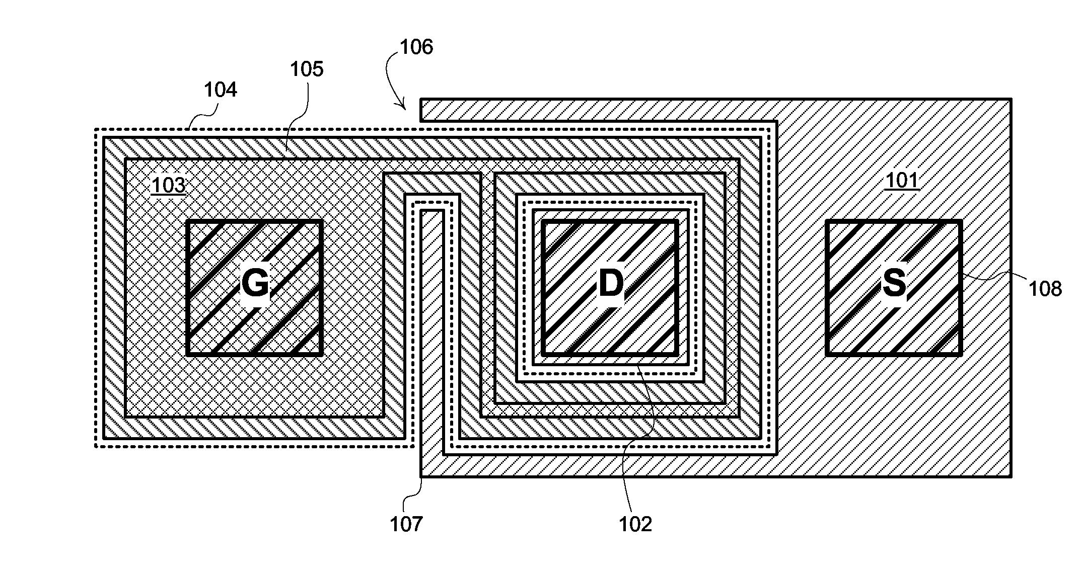
[0063] Specifically, to improve the ruggedness and avalanche capability of a power MESFET, three issues must be addressed in its design and fabrication. The intrinsic weaknesses in present day MESFETs include edge breakdown effects, surface breakdown effects, and lack of a low-impedance voltage clamp in the unipolar MESFET structure itself. Remedies for each of these issues may be applied individually, or in combination, to improve the avalanche ruggedness and robustness of a MESFET to a lev...


PUM


Abstract

A rugged MESFET for power applications includes a drain region surrounded by a ring shaped gate. The gate is surrounded, in turn by a source region. This eliminates the high-field point between gate and drain along the device's etched mesa surface and results in improved avalanche capability.

Description

RELATED APPLICATIONS [0001] This application is one of a group of concurrently filed applications that include related subject matter. The six titles in the group are: 1) High Frequency Power MESFET Gate Drive Circuits, 2) High-Frequency Power MESFET Boost Switching Power Supply, 3) Rugged MESFET for Power Applications, 4) Merged and Isolated Power MESFET Devices, 5) High-Frequency Power MESFET Buck Switching Power Supply, and 6) Power MESFET Rectifier. Each of these documents incorporates all of the others by reference. BACKGROUND OF INVENTION [0002] DC-to-DC conversion and voltage regulation is an important function in virtually all electronic devices today. In low voltage applications, especially thirty volts and less, most switching regulators today use insulated-gate power transistors known as power MOSFETs. Power MOSFETs, despite certain high-frequency efficiency and performance limitations, have become ubiquitous in handheld electronics power by Lilon batteries (i.e. operatin...

Claims


Application Information

Patent Timeline
Patent Type & Authority Applications(United States)
IPC IPC(8): H01L31/112
CPCH01L21/8252H01L27/0605H01L29/0692H01L29/42316H01L29/66878H01L29/8128H01L24/06H01L2224/0603H01L2224/32245H01L2224/48091H01L2224/48464H01L2224/49113H01L2224/73265H01L2924/12032H01L2924/12035H01L2924/13091H01L2224/04042H01L2924/13063H01L2924/14H01L2924/00014H01L2924/00
Inventor WILLIAMS, RICHARD K.NILSSON, JAN
Owner ADVANCED ANALOGIC TECHNOLOGIES INCORPORATED
Why Eureka
Try Eureka