One-time programmable memory

US20070133259A1Inactive Publication Date: 2007-06-14KIM JUHAN
5 Cites 15 Cited by

Patent Information

Authority / Receiving Office
US · United States
Current Assignee / Owner
Publication Date
2007-06-14
Estimated Expiration
Not applicable · inactive patent

Smart Images

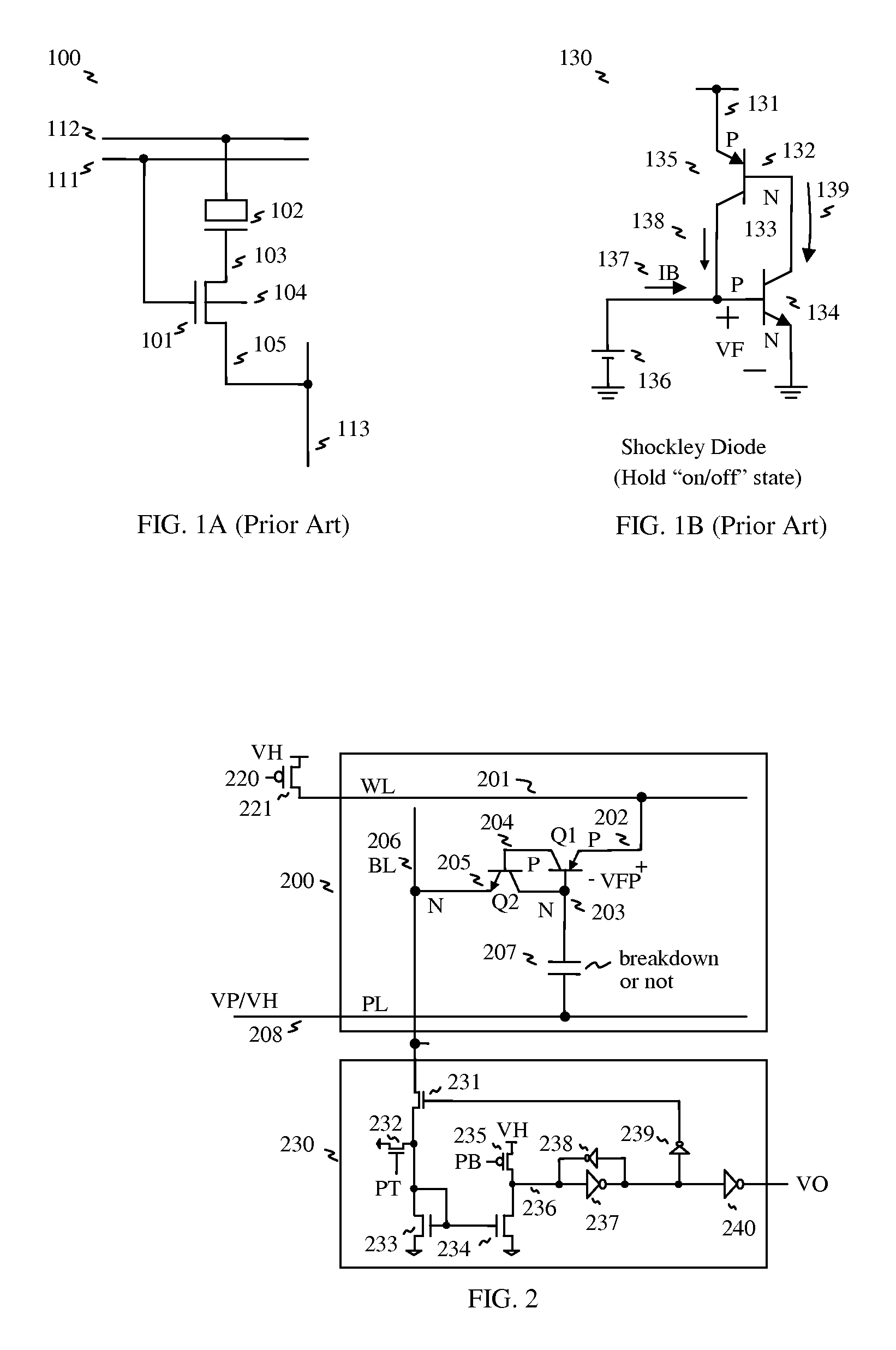
  • Figure 1
    Figure 1
  • Figure 2
    Figure 2
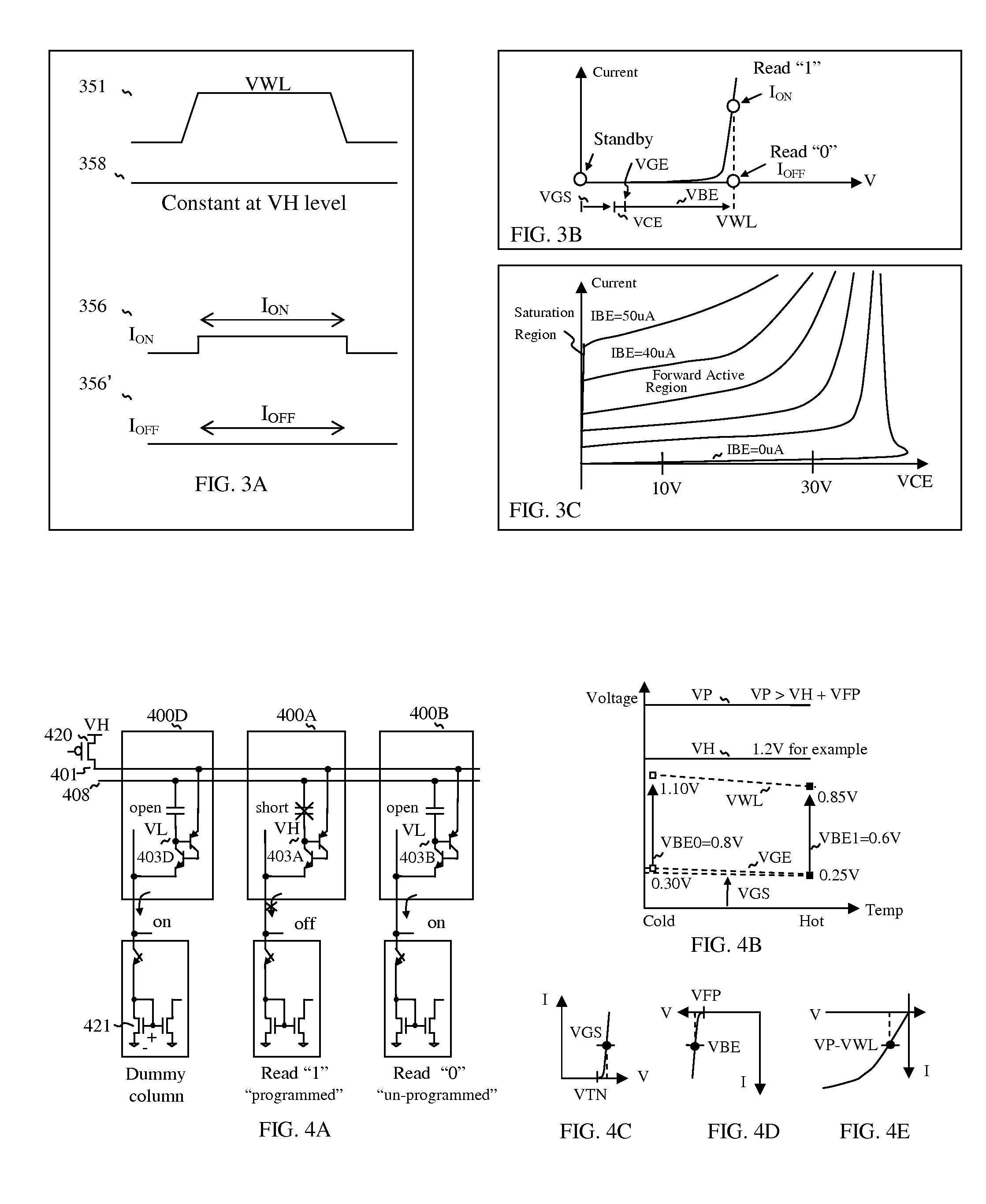
  • Figure 3
    Figure 3
Patent Text Reader

Abstract

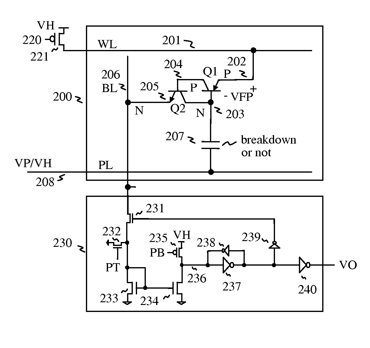
In the present invention, one-time programmable memory includes a diode as an access device and a capacitor as a storage device, the diode includes four terminals, wherein the first terminal is connected to a word line, the second terminal is connected to one plate of the capacitor, the third terminal is floating, and the fourth terminal is connected to a bit line, and the capacitor includes two electrodes, wherein one of the capacitor plate serves as a storage node which is connected to the second terminal of the diode, and another plate of the capacitor is connected to a plate line, and the plate line is asserted to programming voltage which is higher than the regular supply voltage of the decoders and data latches, in order to breakdown the insulator of the capacitor when programming, but the plate line is connected to the regular supply voltage when read. And during read, the diode also serves as a sense amplifier to detect whether the storage node is forward bias or not, and it sends binary data to a latch device wherein includes a current mirror and a feedback loop, which cuts off the current path after latching. And dummy columns generate replica delay signals which guarantee timing margin and reduce cycle time. In addition, the memory cells are formed in between the routing layers, which memory cells can be stacked over the transistor or another capacitor memory cell.
Need to check novelty before this filing date? Find Prior Art

Description

FIELD OF THE INVENTION

[0001] The present invention relates to a semiconductor memory device, and more particularly, to an OTP (One-Time Programmable) memory using a diode as an access device. BACKGROUND OF THE INVENTION

[0002] One-time programmable (OTP) memories are used in integrated circuits for a variety of applications including nonvolatile memory applications. They may be used as a single memory cell, or in arrays of memory cells to provide unique chip identifications and to set operating parameters such as clock multipliers and voltage levels for devices such as microcontrollers and microprocessors, and also high-density memory applications. They may also be used to configure, customize, and repair a chip after testing, in order to repair a controller's cache memory array. One-time programmable memories are typically implemented using charge storage, fuse, or anti-fuse approaches. Charge storage approaches have typically involved defining a bit value based on charge stored o...

Examples

Embodiment Construction

)

[0029] Reference is made in detail to the preferred embodiments of the invention. While the invention is described in conjunction with the preferred embodiments, the invention is not intended to be limited by these preferred embodiments. On the contrary, the invention is intended to cover alternatives, modifications and equivalents, which may be included within the spirit and scope of the invention as defined by the appended claims. Furthermore, in the following detailed description of the invention, numerous specific details are set forth in order to provide a thorough understanding of the invention. However, as is obvious to one ordinarily skilled in the art, the invention may be practiced without these specific details. In other instances, well-known methods, procedures, components, and circuits have not been described in detail so that aspects of the invention will not be obscured.

[0030] Detailed descriptions for the present invention are described as follows, which include th...