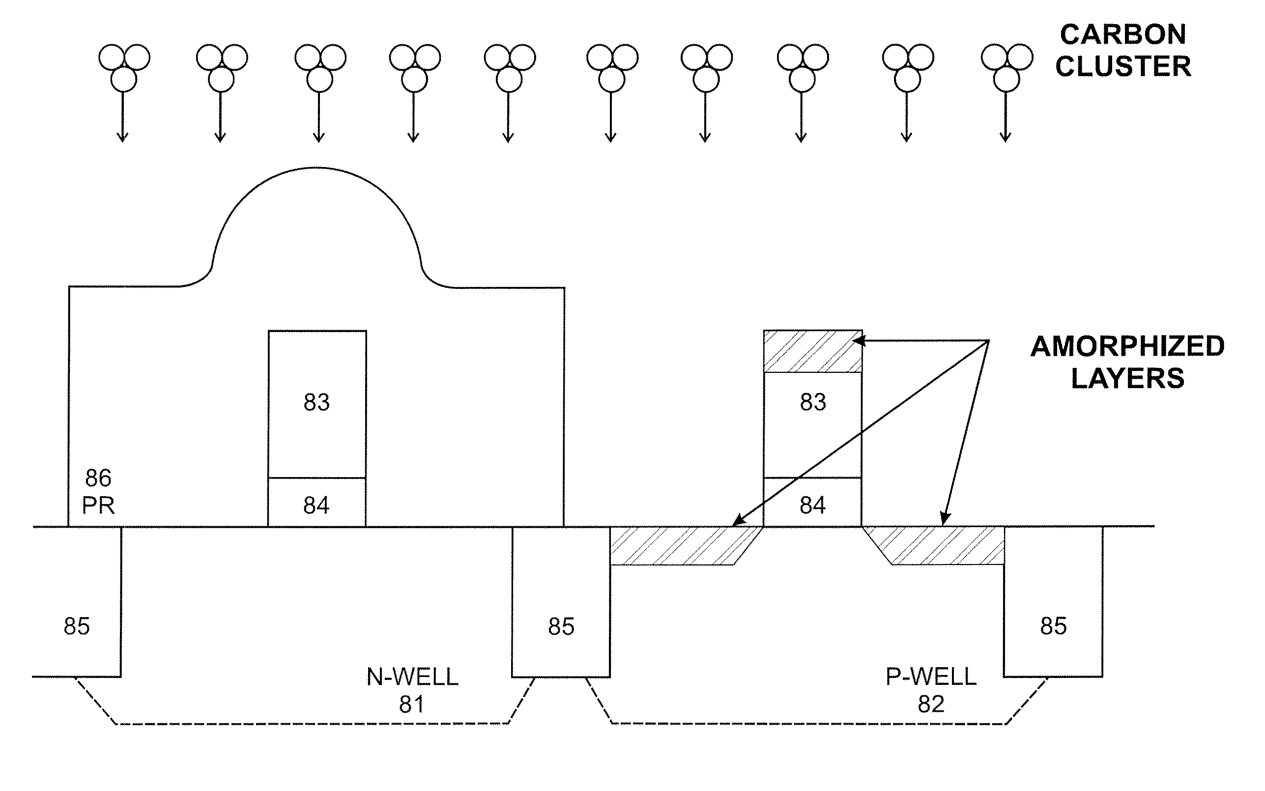
[0019] There is a secondary benefit to the process in accordance with the present invention that is of great economic value; namely, amorphization of the
silicon by the carbon cluster implant and the subsequent boron cluster implant. In particular, it is known in the art that implantation of large boron clusters amorphize the
crystalline silicon lattice, resulting in a large reduction in ion channeling. Channeling is known to significantly increase the
junction depth of a
dopant implant thereby making USJ formation difficult. Channeling is typically controlled by first conducting a damage implant, for example by Ge+ atoms, to amorphise the
silicon prior to forming the PMOS source / drain extensions by implanting boron. The Ge+ implant is expensive to perform, and has also been shown to create defects at its end-of-range which increases leakage currents in the USJ transistors, in certain cases by several orders of magnitude. Thus, replacing the conventional boron implant by a boron cluster, such as B18Hx+, obviates the need for the Ge implant in many cases, and does not generate the defect structures associated with leakage. This is of great economic value since is removes a costly implant from the process flow, increases yield, and reduces leakage current in the integrated circuits. Unfortunately, the boron cluster implant can never entirely eliminate channeling, since before the critical dose for amorphization is reached, a fraction of the boron cluster implant has been performed, and has contributed to a channeling
tail. For example, an 80% reduction in channeling has been demonstrated by the implantation of B18Hx+ ions to form the source / drain extensions, but to achieve the most shallow junctions, a damage implant is still required. If, however, according to the process in accordance with the present invention, a carbon cluster is implanted followed by an implant of either boron clusters or
monomer boron, the silicon has been fully amorphized by the carbon implant, so channeling can be entirely eliminated.
[0027] In addition, when very shallow carbon implants are required, the use of a carbon cluster by the process in accordance with the present invention increases the effective
dose rate (and hence the
wafer throughput) relative to performing
monomer carbon implants, providing a similar increase to
throughput achieved by substituting boron clusters for
monomer boron.
Phosphorus Diffusion Control
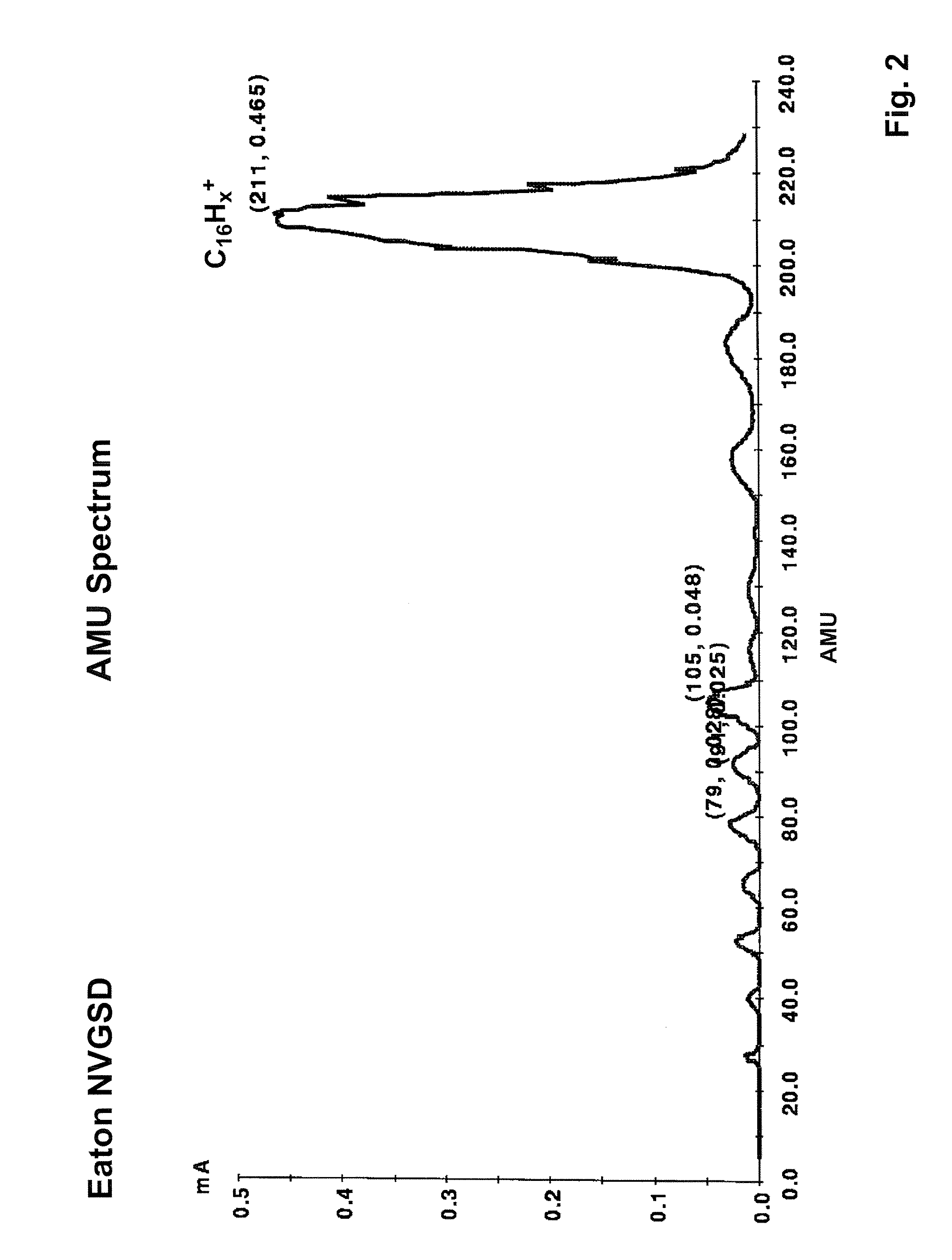
[0037] Flouranthene is the material used to generate much of the data included in this disclosure. In general, any
hydrocarbon with a
chemical formula of the form CnHy, where n≧4 and y≧0 will provide the above features and benefits, namely, increasing the effective carbon
dose rate into the silicon, and providing varying degrees of amorphization, in all cases being more beneficial than a monomer carbon implant.
[0043] As the junction requirements become shallower, the boron implant energy must be reduced. Likewise, the carbon implant energy required to effectively reduce
diffusion must also be reduced. The use of the carbon cluster or molecule enables very
high productivity at very low energies, which is required for advanced technologies. Another critical concern driving the carbon implant process to lower energies is the control of leakage current. Carbon at high concentrations in a junction region is known to endanger
low leakage operation. Since most of the active junction is deeper than the source / drain extension junction, carbon at higher energies gets placed exactly in the region of highest leakage risk. One approach to managing this issue is to keep the carbon cluster as shallow as possible, and minimize the dose. In this way, any enhancement of the
junction leakage current is minimized. Pre-Amorphization
[0046] It has been shown that carbon incorporated into the source / drain regions of the transistor in silicon can form SixCy material which provides a
lattice mismatch to pure silicon and therefore mechanically stresses the
transistor channel, increasing carrier mobility, as discussed in the Ang, et al. reference, mentioned above. The SixCy material has a smaller lattice than the silicon, so this material creates tensile stress in the channel which is useful for improving the mobility of NMOS transistors. As such, in accordance with an important aspect of the invention, carbon cluster implantation, such as with C16H10+, is used to perform high dose implants as the means of converting silicon into SixCy selectively in the source / drain regions of an NMOS transistor. At a given
ion current, the use of a cluster like C16H10 multiplies the carbon dose by a factor of sixteen, and enables ultra shallow implants at high dose

