Low-k dielectric material

a dielectric material and low-k technology, applied in the field of thin films, can solve the problems of reliability failure, increased softness, brittleness and cracking, and high cost of increased softness, and achieve excellent mechanical and thermal properties

Active Publication Date: 2007-08-16
SILECS OY
View PDF4 Cites 13 Cited by
  • Summary
  • Abstract
  • Description
  • Claims
  • Application Information

AI Technical Summary

Benefits of technology

[0023] It is an object of the present invention to eliminate the problems of the known technical solutions and to provide novel low dielectric constant thin films, which have excellent mechanical and thermal properties.

Problems solved by technology

Silicate-based low-k materials can demonstrate exceptional thermal stability and usable modulus but can be plagued by brittleness and cracking.
In contrast, organic materials often show improved material toughness, but at the expense of increased softness, lower thermal stability, and higher thermal expansion coefficients.
Porous materials sacrifice mechanical properties and possess a strong propensity for absorbing chemicals used in semiconductor fabrication leading to reliability failures.
Fluorinated materials can induce corrosion of metal interconnects, rendering a chip inoperative.
Universally, low-k materials sacrifice mechanical robustness and thermal conductivity with respect to their pure silicon dioxide analogues, making integration into the fabrication flow very challenging.
Further, known materials comprising exclusively inorganic bonds making up the siloxane matrix are brittle and have poor elasticity at high temperatures.
However, in spite of advantages achieved by using the known precursors, there are still disadvantages of the known methods of their manufacture.
First, the manufacture of these precursors is inefficient because the chemical reactions have low yields, and the process is expensive and produces toxic byproducts.
Further, it is difficult to eliminate redimerization of the reactive intermediates.
When deposited along with polymers, these dimers decrease the thermal stability and mechanical strength of the film.
Moreover, materials currently reaching dielectric constant less than 2.5 are typically highly porous, which makes the integration of such materials very difficult.
Thus, the prior art contains no examples of dielectric material precursors for semiconductor manufacture, which have desired properties of low dielectric constant with low porosity, high thermal stability, and low cost.

Method used


Image

  • Low-k dielectric material
  • Low-k dielectric material
  • Low-k dielectric material

Examples


example a

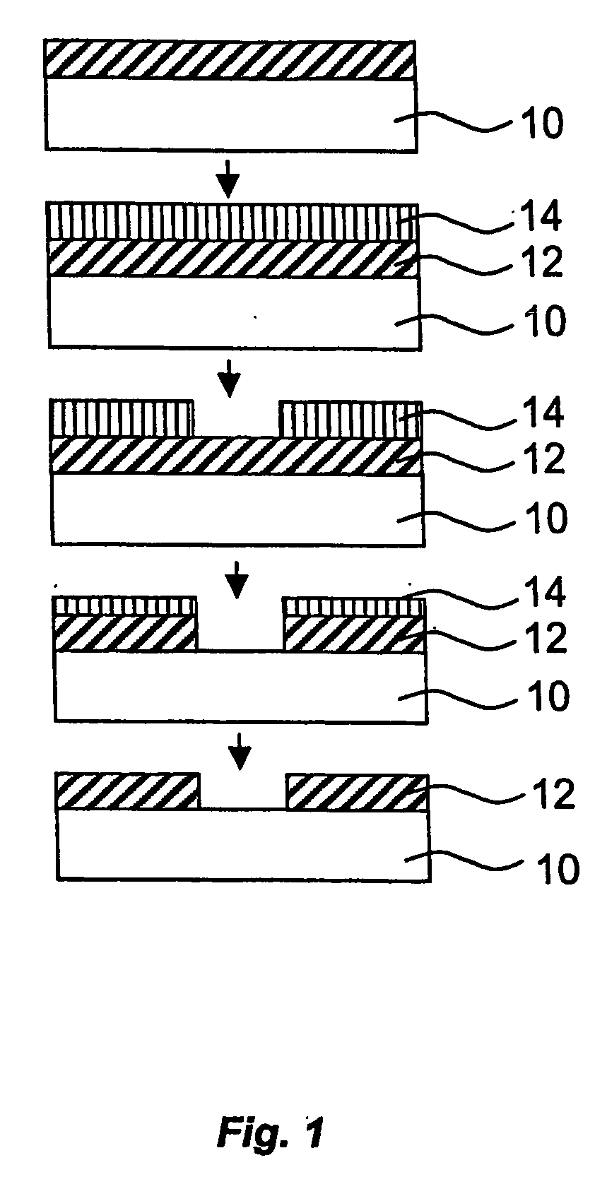
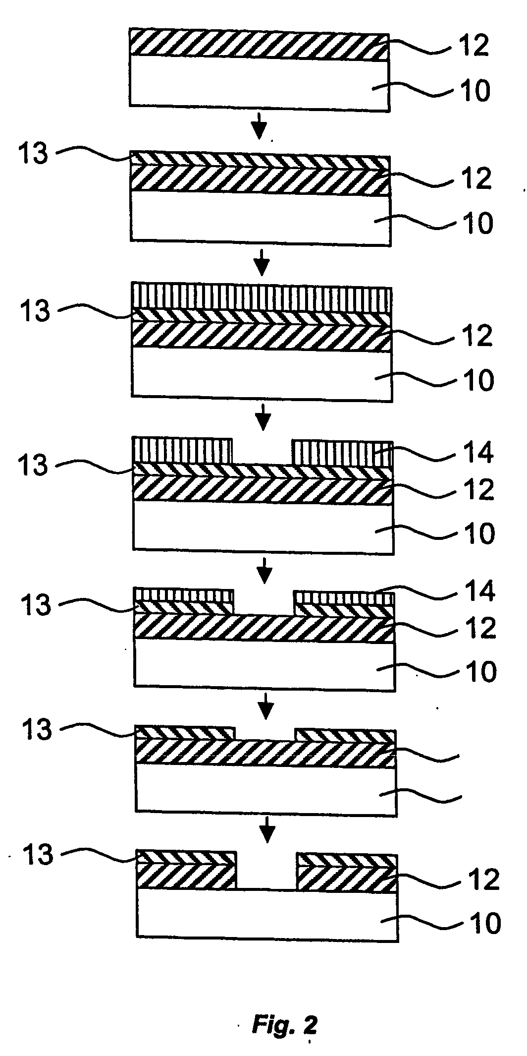
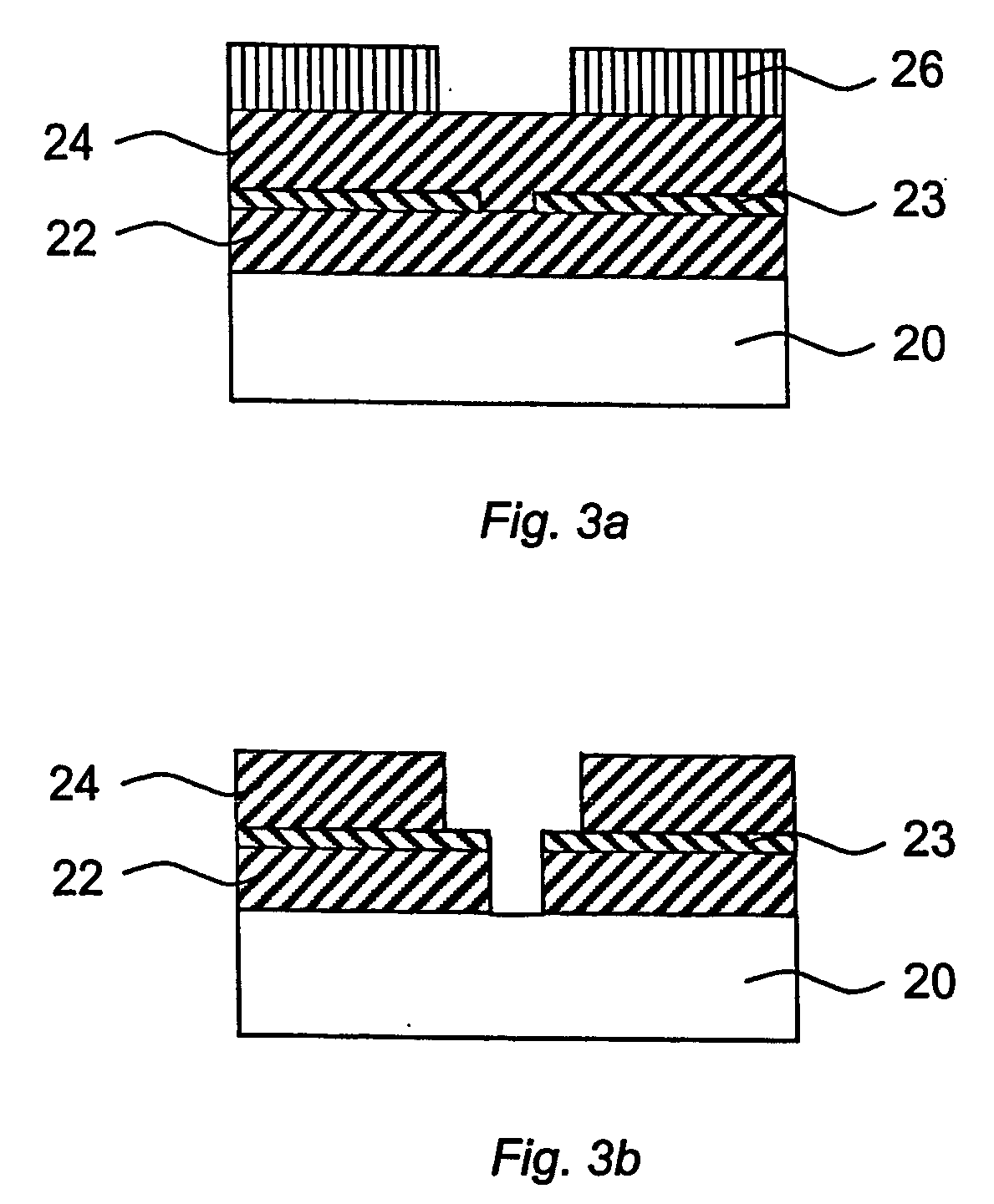
[0109] In one embodiment, the present invention relates to a chemical vapor deposition (CVD) process and more preferably a plasma enhanced chemical vapor deposition (PECVD) process for forming a low-k dielectric thin film on a substrate, including the steps of: placing the substrate in a chemical vapor deposition apparatus, introducing at least one vaporized organosilicon precursor comprising at least one cleavable organic functional group into-the apparatus; transporting the organosilicon- vapor into a chemical vapor deposition zone containing a substrate, optionally using a carrier gas to effect such transport; contacting the organosilicon vapor with the substrate under chemical vapor deposition conditions to deposit a thin film comprising an organosilicon composition; and activating the organosilicon thin film to produce a low-k dielectric thin film. The activation step is carried out under conditions sufficient to effect the removal of at least a portion of the cleavable, organi...

example b

[0111] The materials are deposited as in example A and the formed films are further annealed at elevated temperatures in air, nitrogen, argon, forming gas or vacuum. The curing temperature is preferably higher than the deposition temperature in the deposition step described in the method A and can be as high as 600 deg C. but is not limited to that.

[0112] In this embodiment, the present invention relates to a chemical vapor deposition (CVD) process and more preferably a plasma enhanced chemical vapor deposition (PECVD) process for forming a low-k dielectric thin film on a substrate, including the steps of: placing the substrate in a chemical vapor deposition apparatus, introducing at least one vaporized organosilicon precursor comprising at least one cleavable organic functional group into the apparatus ; transporting the organosilicon vapor into a chemical vapor deposition zone containing a substrate, optionally using a carrier gas to effect such transport; contacting the organosi...

example c

[0114] The materials are deposited as in example A and the formed films are radiation exposed (UV, DUV, Extreme UV, IR or e-beam) prior to further treatments such as curing at elevated temperatures in air, nitrogen, argon, forming gas or vacuum or prior second layer deposition such as metal, barrier, liner or additional dielectric layer deposition, which can be either regular dielectric film, low-k dielectric film or high-k dielectric film. The exposed can be applied through a mask or reticle or alternatively in a flood exposure manner. The exposure step can also be followed by a development step or elevated temperature-curing step.

[0115] Thus, in addition to thermally and plasma-generated reactive intermediates, photon assisted precursor cracking is also part of this invention. Because specific chemical bonds have specific energies, and because these energies can be supplied as photons, electromagnetic radiation is a preferred method of practicing this invention.

[0116] According ...


PUM

PropertyMeasurementUnit
dielectric constantaaaaaaaaaa
pressureaaaaaaaaaa

Abstract

Method for forming a low dielectric constant structure on a semiconductor substrate by CVD processing. The method comprises using a precursor containing chemical compound having the formula of (R1—R2)n-Si—(X1)4-n, wherein X1 is hydrogen, halogen, acyloxy, alkoxy or OH group, R2 is an optional group and comprises an aromatic group having 6 carbon atoms and R1 is a substituent at position 4 of R2 selected from an alkyl group having from 1 to 4 carbon atoms, an alkenyl group having from 2 to 5 carbon atoms, an alkynyl group having from 2 to 5 carbon atoms, Cl or F; n is an integer 1-3. The present precursors allow for a lowering of the electronic dielectric constant compared to conventional dielectric materials, such as silicon dioxide or phenyl modified organo-containing silicon dioxide.

Description

BACKGROUND OF THE INVENTION [0001] 1. Field of the Invention [0002] The present invention relates to thin films suitable as dielectrics in IC's and for other similar applications. In particular, the invention concerns thin films comprising compositions obtainable by hydrolysis and / or condensing of one or more silicon compounds, which yield an at least partially cross-linked siloxane structure via chemical vapor deposition (CVD) methods. The invention also concerns a method for producing such films by preparing siloxane compositions by CVD deposition of suitable reactants, by applying the hydrolyzed compositions on a substrate in the form of a thin layer and by optional curing the layer to form a film. [0003] 2. Description of Related Art [0004] Built on a semiconducting substrate, integrated circuits comprise of millions of transistors and other devices, which communicate electrically with one another and outside packaging material through multiple levels of vertical and horizontal ...

Claims


Application Information

Patent Timeline
Patent Type & Authority Applications(United States)
IPC IPC(8): H01L21/31C23C16/40H01L21/312
CPCC07B2200/11C07F7/1836C23C16/401C23C16/56H01L21/31633H01L21/02216H01L21/02274H01L21/02277H01L21/02345H01L21/02126C07F7/1804
Inventor RANTALA, JUHA T.
Owner SILECS OY
Why Eureka
Try Eureka