[0039] In addition to the cost
advantage of the present invention, the resulting alignment layers and wafers produced using the teachings of the present invention offer several functional advantages over conventional alignment layers. Specifically, the alignment layers formed using the present invention can be made thinner and are more uniform than conventional alignment layers. For example, using the process of the present invention, alignment layers can be made as thin as 5 to 50 Angstroms as opposed to 800 to 3000 angstroms for conventional alignment layers. Very thin alignment layers have many advantages over the thicker PI alignment layers, for example, the
voltage drop across the alignment layer is significantly lower in a thin alignment layer. In addition, the thin alignment layer does not require a PI alignment
mask, which are very expensive. Furthermore, the chance of
contamination is greatly reduced by using vapor deposition rather than liquid coatings.
[0041] The
substrate surface material also plays an important role on the coated film
adhesive strength on the substrate surface. In general,
silicon based materials, such as SiO2 (
silicon dioxide), SiO (
silicon monoxide) and SiOx (
silicon Oxide), Si3N4, SiNx (
silicon nitride), and SiOxNy (
silicon oxynitride), are excellent materials with good
adhesive strength to the
silane material. Thus, a
thin layer of these materials is a suitable material as the substrate surface materials for embodiments of the present invention. For example, in one embodiment of the present invention a thin adhesion layer is deposited over the substrate coated with ITO layer to promote the
silane material
coating on the ITO substrate surface. The thin adhesion layer can be any of the silicon-based materials described above.
[0042] While using a specialized Vacuum-bake / vapor prime
coating machines as described above provides many advantages, embodiments of the present invention can also be carried out in less sophisticated equipment. For example conventional equipment used to deposit HMDS (Hexamethyldisilazane) (as the photo
resist adhesive
promoter) in conventional photo
resist processes can be used to implement some embodiments of the present invention. The LPCVD (low pressure
chemical vapor deposition) process or a simple vapor
deposition process is used for the HMDS deposition. However, HMDS is not used as the LC alignment layer for the MVALCDs because HMDS produces a parallel, non-vertical, LC alignment layers. Furthermore, HMDS does not adhere to ITO layer. However, the process used to deposit HMDS can be used to deposit other silane materials with corresponding pressures, temperature, and time adjustments.
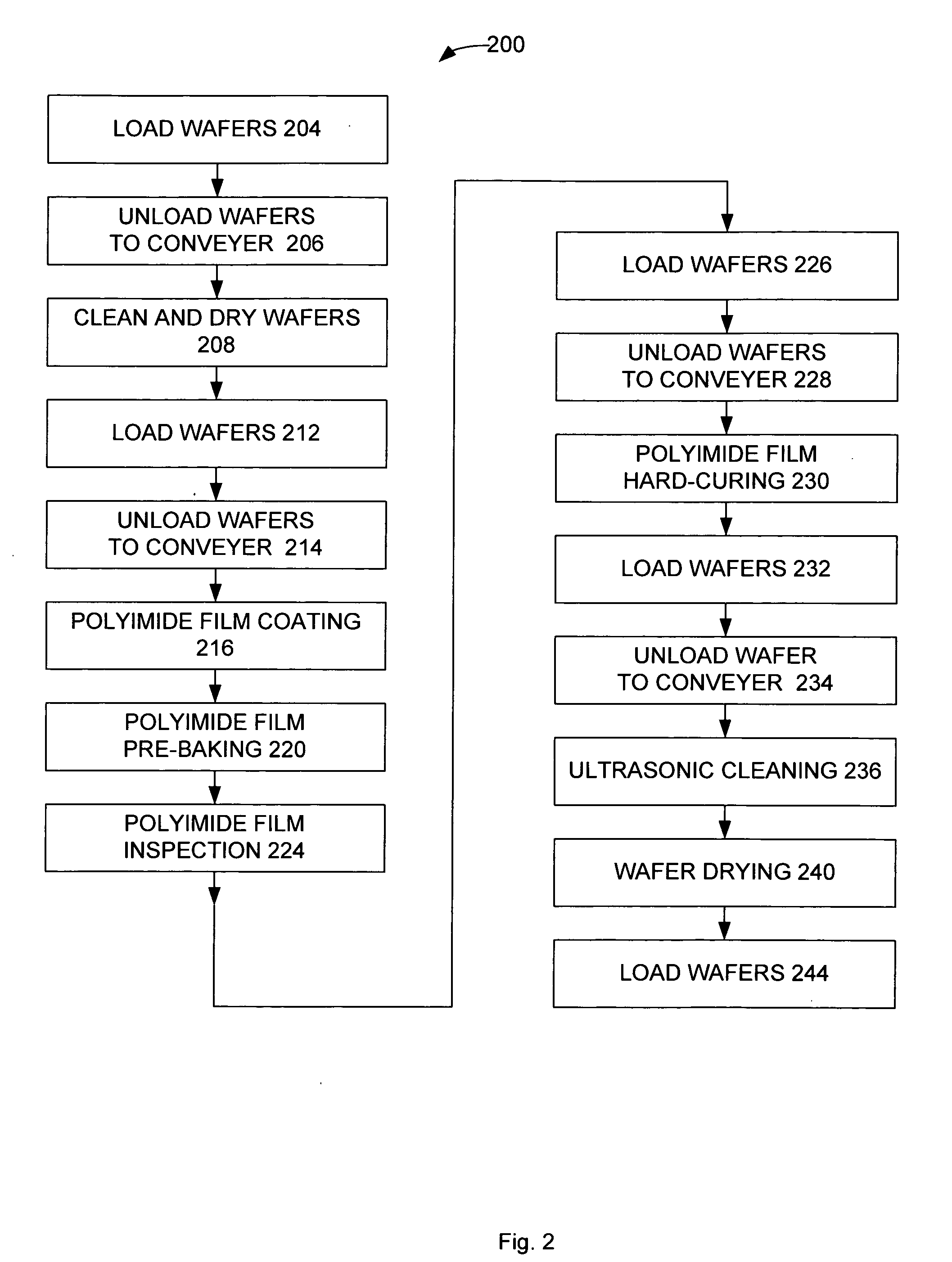
[0043]FIG. 4 is a
process flow diagram of a novel process 400a to fabricate a liquid
crystal alignment layer for MVALCD in accordance with one embodiment of the present invention. Novel process 400a can performed using a conventional equipment, such as the HMDS deposition system from Tokyo Ohka Kogyo CO., LTD, of Tokyo, Japan, Active CO., LTD of Sakitama, Japan, Tokyo
Electron of Tokyo, Japan; and Aviza Technology of San Francisco, Calif. In general, the HMDS deposition systems processes wafers serially, that is, the HMDS deposition systems performs the silane vapor deposition serially. Additional equipment is used to perform hard curing as a batch process.
[0044] Novel Process 400a is similar to novel process 300a; however, due to limitations of conventional equipment additional steps are necessary to properly cure the alignment layers. The wafers are initially loaded into a Cassette in LOAD WAFERS INTO CASETTE 402. Then the wafers are unloaded serially onto a conveyer, which will load the wafers serially into a vacuum chamber, in UNLOAD WAFERS TO CONVEYER 404. In
VACUUM CHAMBER PURGE 308, a vacuum chamber purge process is performed to completely remove
water vapor that may be present in the vacuum chamber or the wafers. Specifically, the vacuum chamber is evacuated to a low pressure, such as 10-30 millitorrs, and refilled with a pre-heated
inert gas, such as
nitrogen, at a temperature of 80-200° C. The evacuation / refilling with
nitrogen can be repeated several times to insure complete removal of
water vapor from the vacuum chamber. Furthermore, due to the preheated
inert gas and by the thermal
heating element in the oven, the wafers are brought to a temperature that facilitates vapor deposition (as described below).

