Mold for photocuring nano-imprint and its fabrication process

a technology of nano-imprints and molds, which is applied in the field of molds for photocuring nano-imprints and their fabrication processes, can solve the problems of high cost of systems used with such photolithography, difficult to form the desired pattern, and expensive fabrication technologies, and achieves the effect of improving robustness and high releasability

Inactive Publication Date: 2007-11-22
DAI NIPPON PRINTING CO LTD
View PDF8 Cites 38 Cited by
  • Summary
  • Abstract
  • Description
  • Claims
  • Application Information

AI Technical Summary

Benefits of technology

[0023] In view of such problems as mentioned above, an object of the invention is to provide a mold for photocuring nano-imprint having a high releasibility with respect to a photocuring (photocured) resin and an improved robustness, and its fabrication process.
[0029] The photocatalytic substance here, for instance, is photocatalytic titanium oxide. Meant by the photo-catalytic titanium oxide is one of titanium oxide species that has a crystal structure. Non-crystal type titanium oxide is inadequate in terms of photocatalytic performance. The photocatalytic titanium oxide generates, upon irradiation with light of a wavelength having an energy greater than its band gap, electrons at a conduction band and positive holes at a valence band by way of photo-excitation. The electrons generated by that photo-excitation have a strong reducing power, and the positive holes have a strong oxidizing power: both have an effect on the decomposition, and purification of organic matter or the like.
[0031] Therefore, if a photocatalytic titanium oxide film is formed on the surface of the mold for photocuring nano-imprint, it is then possible to prevent sticking of the photocured resin onto the surface of the mold, because it is exposed to ultraviolet light for each pattern transfer process; that is, even when the photocuring resin is pressed onto the mold, the power of binding organic matter (photocured resin) to the surface of the mold is permitted to wane by way of the photocatalytic effect so that the sticking of the photocured resin onto the surface of the mold can be prevented.
[0032] The organic substance that is decomposed by the photocatalytic titanium oxide with such irradiation of light as mentioned above, for instance, includes organic halogen compounds, organic phosphorus compounds, hydrocarbons such as surfactants or oils, aldehydes, mercaptans, alcohols, amines, amino acids, and proteins. Thus, the photocatalytic titanium oxide film exhibits a high releasability for the photocured resin that is an organic substance but a low releasability for quartz or glass that is an inorganic substance. With the photo-catalytic titanium oxide film, therefore, the problem with the fluororesin coating film that comes to peel off would be eliminated.
[0039] By the provision of that electrically conductive layer, inconveniences caused by electrification by electron beam irradiation, for instance, changes in the size and position of the desired pattern can be eliminated.
[0045] According to the invention as described above, it is possible to provide a mold for photocuring nano-imprint that has an improved releasability for the photocuring (photocured) resin and an improved robustness as well, and its fabrication process.

Problems solved by technology

However, systems used with such photolithography costs much, and less costly fabrication technologies are still in need.
A problem here is that when the NIL mold 20 is taken off from the state with the NIL mold 20 pressed onto the resin as depicted in FIG. 8(b), there is the photocured resin 33 remaining partly stuck onto the NIL mold 20, as shown in FIG. 9, with the result that it becomes difficult to form the desired pattern.
A problem with coating the fluororesin onto the NIL mold 20 is, however, that there is no adequate adhesion between the NIL mold 20 and the fluororesin.
Problems with coating by dipping are, on the other hand, that the coated film becomes uneven, robustness drops due to the aforesaid peeling-off, or the like.

Method used


Image

  • Mold for photocuring nano-imprint and its fabrication process
  • Mold for photocuring nano-imprint and its fabrication process
  • Mold for photocuring nano-imprint and its fabrication process

Examples


example 1

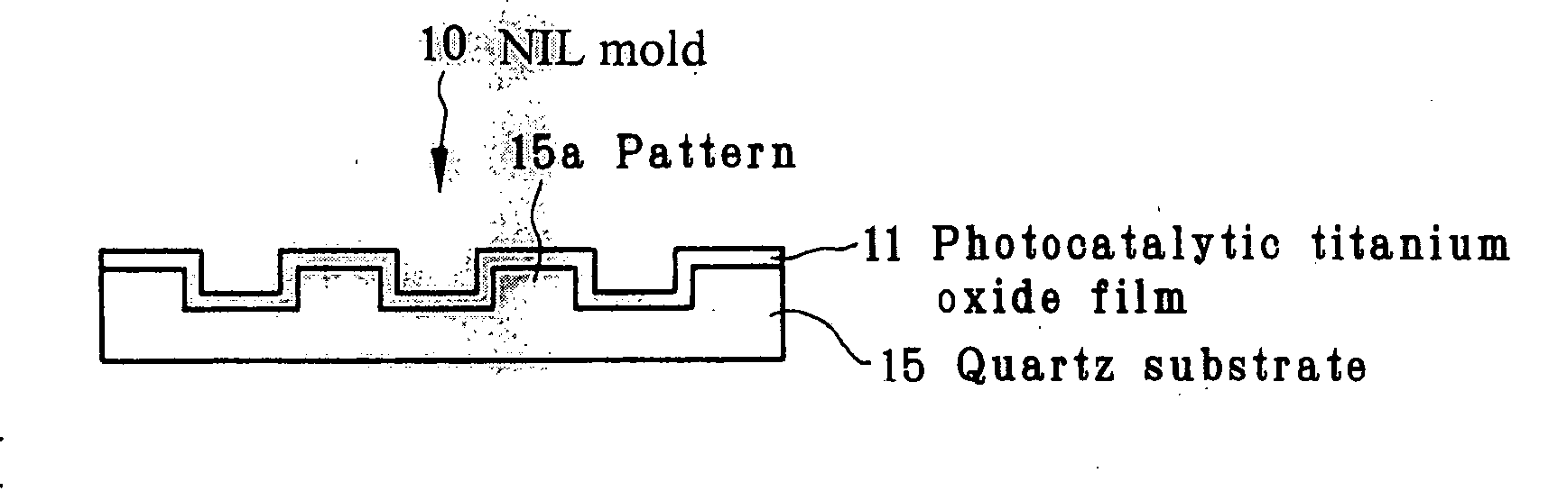
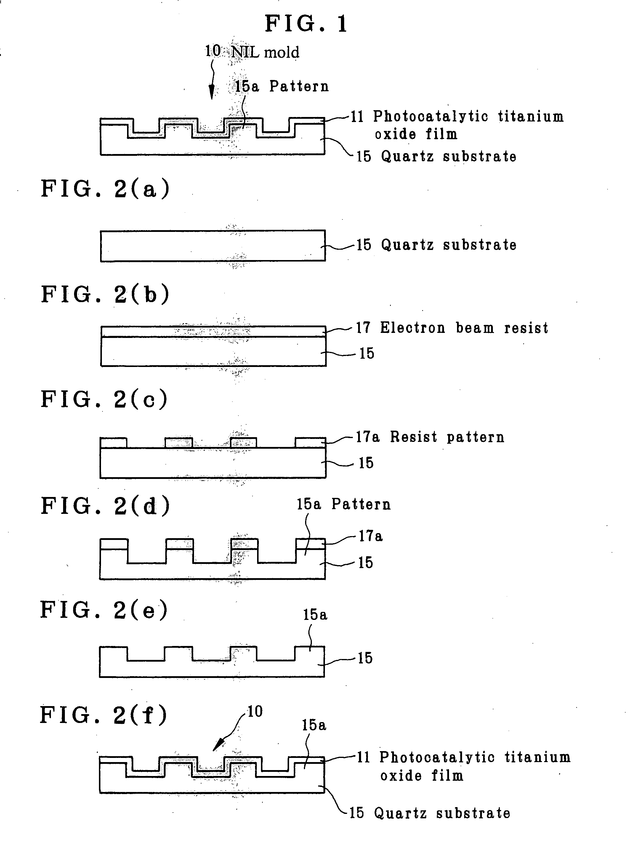
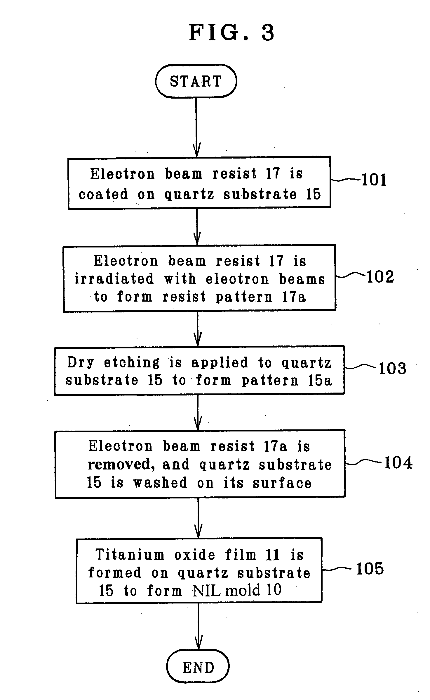
[0078] A novolac resin type electron beam resist (ZEP-520 made by ZEON Co., Ltd.) is coated at a thickness of 100 nm on the surface of a cuboidal quartz substrate having an outside shape of 6 inches in length, 6 inches in width and 0.25 inch in height, then subjected to electron beam lithography, and finally developed to form a line form of resist pattern having a line width of 70 nm.

[0079] Then, carbon tetrafluoride (CF4) is used as etching gas to dry etch the quartz substrate, after which an unnecessary portion of the electron beam resist is ashed off by oxygen gas to obtain a pattern of three-dimensional configuration having a width of 70 nm and a depth of 100 nm.

[0080] Then, sputtering is carried out using a titanium target as the target and argon and oxygen as the sputtering gas at an input power density of 7 W / cm2, after which sintering is done at 400° C. to obtain a photocatalytic titanium oxide film of 5 nm, in thickness, thereby obtaining a mold according to the invention...

example 2

[0083] Cr was sputtered at a thickness of 10 nm on the surface of a cuboidal quartz substrate having an outside shape of 6 inches in length, 6 inches in width and 0.25 inch in height. Afterwards, a novolac resin type electron beam resist (ZEP-520 made by ZEON Co., Ltd.) was coated at a thickness of 100 nm, then subjected to electron beam lithography, and finally developed to form a line-and-space form of resist pattern having a width of 70 nm and a pitch of 140 nm.

[0084] The provision of Cr as the electrically conductive layer makes sure an antistatic effect so that the formed line-and-space resist pattern has the desired values in terms of size and position.

[0085] Then, carbon tetrafluoride (CF4) is used as etching gas to dry etch the quartz substrate, after which an unnecessary portion of the electron beam resist is ashed off by oxygen gas and Cr is removed by a chlorine type gas to obtain a line-and-space pattern of three-dimensional configuration having a width of 70 nm, a pit...


PUM

PropertyMeasurementUnit
wavelengthaaaaaaaaaa
wavelength rangeaaaaaaaaaa
thicknessaaaaaaaaaa

Abstract

The invention relates to a mold that has an improved releasability for a photocured resin and an improved robustness. First, an electron beam resist 17 is coated on a quartz substrate 15 having the nature of being transmissive to ultraviolet light. A resist pattern 17a is formed by irradiation with electron beams. Thereafter, the quartz substrate is dry etched using etching gas such as carbon tetrafluoride to form a pattern 15a on the quartz substrate 15. A photocatalytic titanium oxide film 11 is formed as by sputtering on the surface of the quartz substrate 15 with the pattern 15a formed on it to fabricate an NIL mold 10.

Description

BACKGROUND OF THE INVENTION [0001] The present invention relates to a mold for photocuring nano-imprint and its fabrication process. [0002] With the remarkable progress of microfabrication, as fine as 100 nm resolution is now achievable by photolithography, and so is as fine as 10 nm resolution with electron beams. However, systems used with such photolithography costs much, and less costly fabrication technologies are still in need. For this reason, the formation of desired circuit patterns or the like on silicon or other substrates is being attempted using a nano-imprint technology that is adapted to embody much finer structure than could be possible with a conventional press technology. With this technology, there is in itself no limit to resolution, and the resolution is determined depending on the fabrication precision of a mold. That is, only if a reasonable mold can be fabricated, it would then be possible to form ultra-fine structure more easily than could be possible with c...

Claims


Application Information

Patent Timeline
Patent Type & Authority Applications(United States)
IPC IPC(8): B29D11/00G03C5/00
CPCB29D11/00B82Y10/00G03F7/0017G03F7/0002B82Y40/00
Inventor MORIMOTO, KENICHI
Owner DAI NIPPON PRINTING CO LTD
Why Eureka
Try Eureka