Optical Device and Method of Fabricating the Same

a technology of optical devices and fabrication methods, applied in the field of optical devices, can solve the problems of low work function values, difficult hole injection, and difficult realization of leds with high external quantum efficiency (eqe), and achieve the effect of improving the ohmic contact characteristic and high efficiency

Active Publication Date: 2008-10-23
SAMSUNG DISPLAY CO LTD +1
View PDF4 Cites 48 Cited by
  • Summary
  • Abstract
  • Description
  • Claims
  • Application Information

AI Technical Summary

Benefits of technology

[0027]According to the present invention, an ohmic contact characteristic can be improved by employing t...

Problems solved by technology

The above oxides have relatively low work function values and represent characteristics of suddenly lowering light transmittance at wavelength bands of a visible ray and an ultraviolet ray, so problems occur when the above oxides are used for transparent electrodes of the nitride LED.
First, since conventional TCO or transparent conducting nitride (TCN) has a work function value which is significantly lower than that of a p-type nitride-based cladding layer, if the TCO or TCN is used as a p-type ohmic contact layer, a high energy barrier is formed at an interfacial surface against the carrier flow, so hole injection is very difficult.
For this reason, realizing an LED having high external quantum efficiency (EQE) is very difficult.
In addition, since conventional TCO or TCN does not flexibly match with the electric characteristics formed at the surface of an n-type nitride-based cladding layer, if the TCO or TCN is used as an n-type nitride-based schottky or an ohmic contact electrode structure, the controlling and injecting of holes relative to the carrier flow may be difficult.
For this reason, realizing a light receiving diode or an LED having high light receiving efficiency or high external quantum efficiency (EQE) is very difficult.
In detail, the TCO or TCN represents low light transmittance against light having a wavelength band equal to or lower than that of a blue light, so the TCO or TCN is not suitable for to an LED that emits a light having a short wavelength.
Third, since conventional TCO or TCN has a great light reflective index approximating to 2, emitting the light to an atmosph...

Method used


Image

  • Optical Device and Method of Fabricating the Same
  • Optical Device and Method of Fabricating the Same
  • Optical Device and Method of Fabricating the Same

Examples


first embodiment

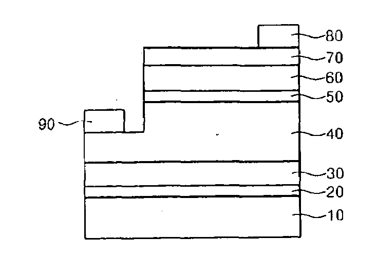
[0043]FIG. 1 is a sectional view showing a top-emitting light emitting diode (TELED) having a p-type multi ohmic contact electrode structure according to the present invention, and FIG. 2 is a sectional view showing a top-emitting light emitting diode (TELED) having a p-type multi ohmic contact electrode structure according to a second embodiment of the present invention.

[0044]In detail, FIG. 1 shows the III nitride-based TELED stacked / grown on a sapphire substrate 10, which is an insulating growth substrate, and FIG. 2 shows the III nitride-based TELED formed on a conductive substrate including silicon carbide (SiC), zinc oxide (ZnO), silicon (Si), gallium arsenic (GaAs), a metal, such as copper (Cu), nickel (Ni) or aluminum (Al), or an alloy formed through electroplating or a bonding transfer scheme.

[0045]Referring to FIGS. 1 and 2, the III nitride-based TELED includes a substrate 10 on which a low-temperature nucleation layer 20, a nitride-based buffer layer 30, an n-type nitride...

third embodiment

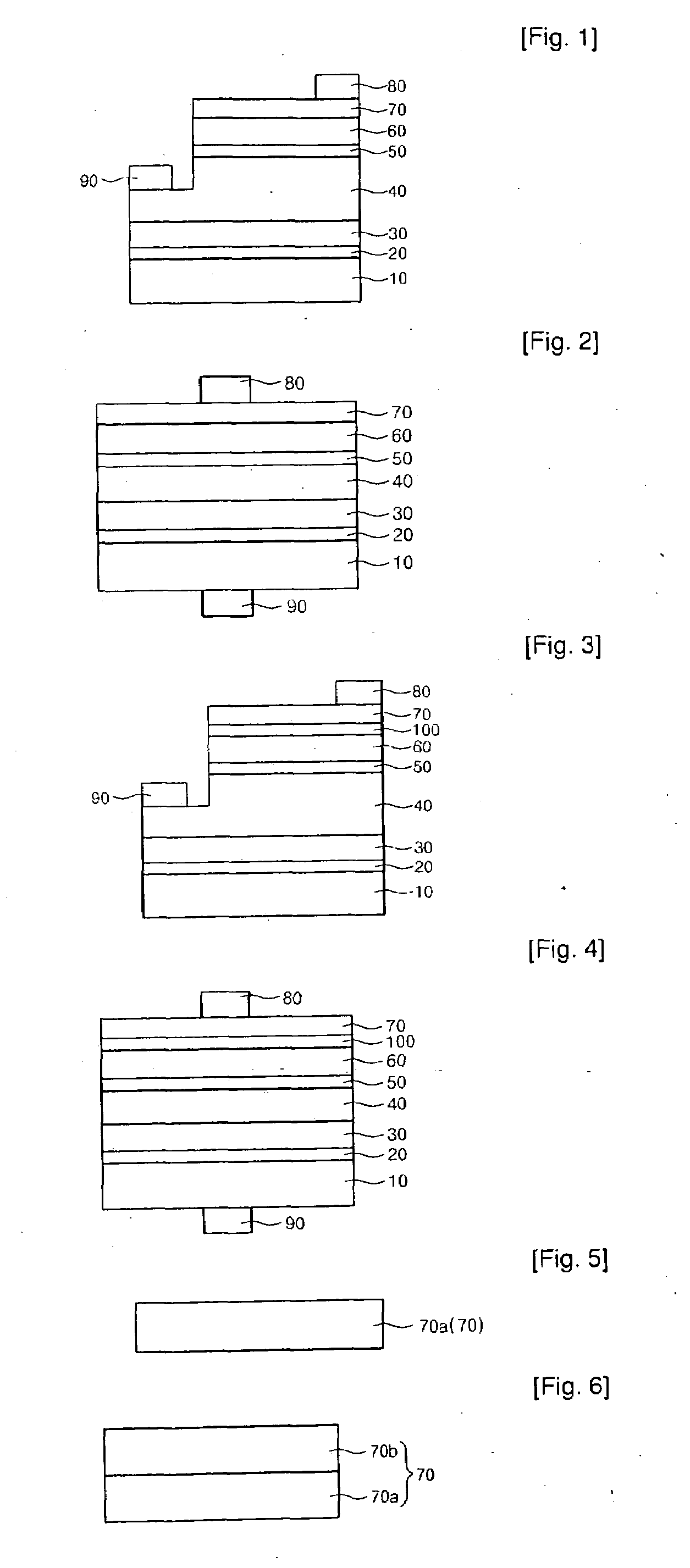
[0061]FIG. 3 is a sectional view showing a top-emitting light emitting diode (TELED) having a p-type multi ohmic contact electrode structure according to the present invention, and FIG. 4 is a sectional view showing a top-emitting light emitting diode (TELED) having a p-type multi ohmic contact electrode structure according to a fourth embodiment of the present invention.

[0062]In detail, FIG. 3 shows the III nitride-based TELED stacked / grown on a sapphire substrate 10, which is an insulating growth substrate, and FIG. 4 shows the III nitride-based TELED formed on a conductive substrate including silicon carbide (SiC), zinc oxide (ZnO), silicon (Si), gallium arsenic (GaAs), a metal, such as copper (Cu), nickel (Ni) or aluminum (Al), or an alloy formed through electroplating or a bonding transfer scheme.

[0063]Different from the first and second embodiments of the present invention, the third and fourth embodiments of the present invention provide a stack structure in which a tunnel ju...

seventh embodiment

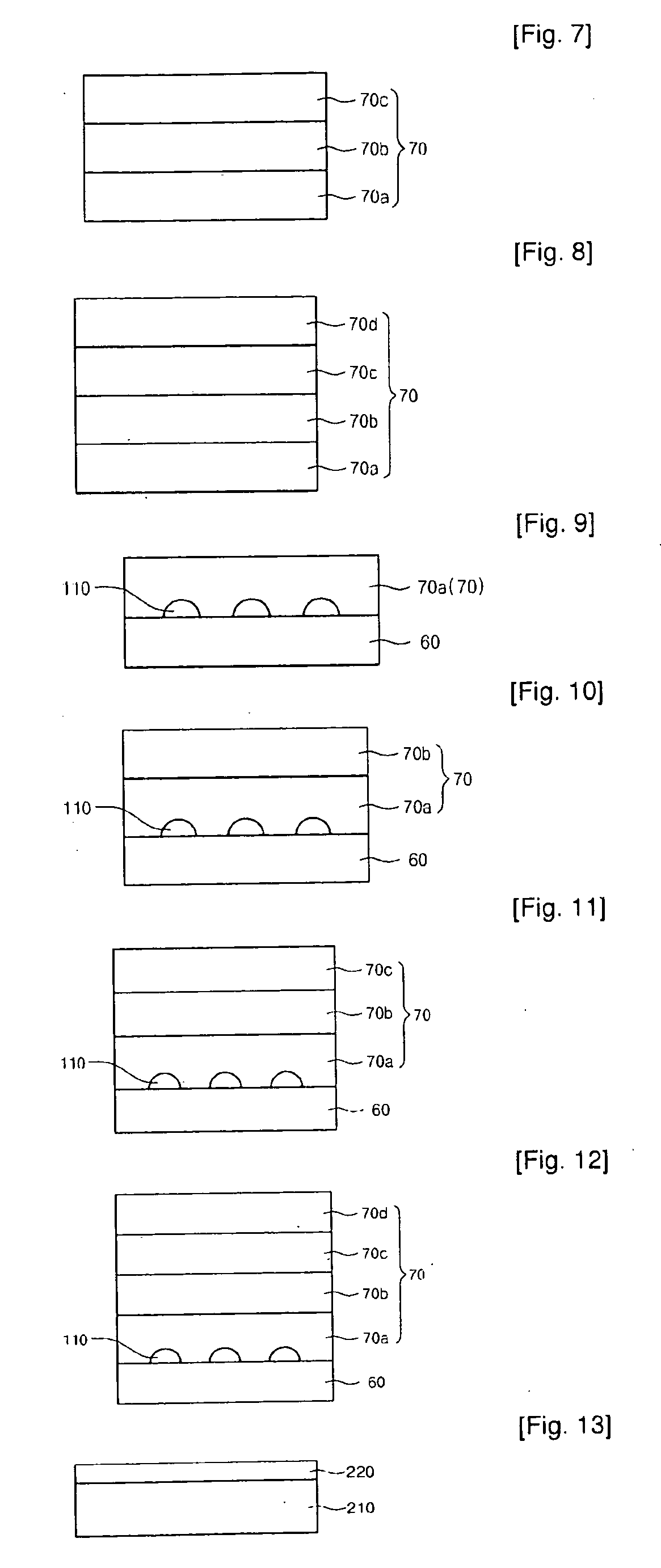
[0092]FIG. 15 is a sectional view showing a structure of a highly transparent n-type multi ohmic contact layer formed on an n-type nitride-based cladding layer according to the present invention, and FIG. 16 is a sectional view showing a structure of a highly transparent n-type multi ohmic contact layer formed on an n-type nitride-based cladding layer according to an eighth embodiment of the present invention.

[0093]In detail, FIG. 15 shows the highly transparent n-type multi ohmic contact layer 240 directly formed on the n-type nitride-based cladding layer 360, and FIG. 16 shows the highly transparent n-type multi ohmic contact layer 240 formed on the n-type nitride-based cladding layer 360 while interposing a tunnel junction layer 380 therebetween.

[0094]The seventh embodiment corresponds to the fifth embodiment and the eighth embodiment corresponds to the sixth embodiment, so detailed description for the same elements will be omitted below in order to avoid redundancy.

[0095]Referri...


PUM


Abstract

Disclosed is an optical device including an optical member and a contact layer stacked on at least one of top and bottom surfaces of the optical member. The contact layer has at least one transparent conducting oxynitride (TCON) layer. The TCON consists of at least one of indium (In), tin (Sn), zinc (Zn), cadmium (Cd), gallium (Ga), aluminum (Al), magnesium (Mg), titanium (Ti), molybdenum (Mo), nickel (Ni), copper (Cu), silver (Ag), gold (Au), platinum (Pt), rhodium (Rh), iridium (Ir), ruthenium (Ru), and palladium (Pd).

Description

TECHNICAL FIELD[0001]The present invention relates to an optical device. More particularly, the present invention relates to an optical device having high efficiency and a method of fabricating the same.BACKGROUND ART[0002]Recently, transparent conducting thin films are used in various fields, such as optoelectronic fields, display fields and energy industrial fields using organic and inorganic materials. In the field of semiconductor light emitting devices including light emitting diodes and laser diodes, materials having superior electrical and optical characteristics must be used in order to promote carrier injection and current spreading and to facilitate emission of photons generated from an active layer of a semiconductor light emitting device.[0003]Many domestic and foreign institutes related to group III nitride light emitting diodes (III nitride LEDs), which are spotlighted as next-generation light sources for illumination, have actively studied to develop transparent condu...

Claims


Application Information

Patent Timeline
IPC IPC(8): H01L29/40H01L21/283H01L33/06H01L33/32H01L33/42
CPCH01B1/08H01L31/022466H01L33/32H01L33/42
Inventor SEONG, TAE-YEON
Owner SAMSUNG DISPLAY CO LTD
Why Eureka
Try Eureka