Methods to mitigate plasma damage in organosilicate dielectrics

a technology of organosilicate dielectrics and plasma damage, which is applied in the direction of basic electric elements, electrical equipment, semiconductor devices, etc., can solve the problems of increasing the overall speed of operation of the advanced semiconductor chips approaching a limit, and the increase of the width of the line trench, so as to reduce the plasma damage, and eliminate the effect of a plasma damaged region

Inactive Publication Date: 2009-03-19
ADVANCED MICRO DEVICES INC +1
View PDF22 Cites 56 Cited by
  • Summary
  • Abstract
  • Description
  • Claims
  • Application Information

AI Technical Summary

Benefits of technology

[0036]The present invention addresses the needs described above by minimizing or eliminating plasma damage to low k and ultra low k organosilicate intermetal dielectric layers. The reduction of the plasma damage is effected by interrupting the etch and strip process flow at a suitable point to add an inventive treatment which protects the intermetal dielectric layer from plasma damage during the plasma strip process. Reduction or elimination of a plasma damaged region in this manner also enables reduction of the line width bias between a line pattern in a photoresist and a metal line formed therefrom, and changes in the line width of the line trench due to a wet clean after the reactive ion etch employed for formation of the line trench and a via cavity. The reduced line width bias has a beneficial effect on electrical yields of a metal interconnect structure.
[0038]In a first embodiment, a silylation reaction is employed to perform a surface treatment and as a consequence to form a modified surface layer, which is a protective layer that protects the material of a patterned intermetal dielectric (IMD) layer from plasma damage during a subsequent plasma strip process. The protective layer is selectively formed on exposed surfaces of the patterned IMD layer, while not modifying the photoresist or a disposable via fill plug in any substantial way. The protective layer shields the patterned IMD layer underneath during the plasma strip process so that plasma damage to the patterned IMD layer is reduced or eliminated.
[0039]In a variation of the first embodiment, a low power and low temperature plasma based deposition process is employed to selectively form a protective layer on exposed surfaces of the patterned IMD layer, while not coating the photoresist or the disposable via fill plug. The protective layer shields the patterned IMD layer underneath during the plasma strip process so that plasma damage to the patterned IMD layer is reduced or eliminated.
[0040]In a second embodiment, a sacrificial layer is formed on exposed surfaces of a patterned IMD layer. The sacrificial layer is consumed during a plasma strip process. However, plasma damage to the patterned IMD layer is reduced or eliminated due to the sacrificial layer.
[0047]performing a plasma strip to remove the disposable via fill material, while the protective layer protects the intermetal dielectric layer from damage during the plasma strip.
[0080]performing a plasma strip to remove the disposable via fill material, while portions of the intermetal dielectric layer underneath the sidewalls and the bottom surface of the line trench and underneath sidewalls of an upper portion of the via hole are protected by the sacrificial layer from damage during the plasma strip, wherein the sacrificial layer is consumed during the plasma strip.

Problems solved by technology

With the progress in the semiconductor device technology leading to ultra large scale integration, the overall speed of operation of the advanced semiconductor chips is approaching a limit due to signal propagation delay in interconnection wires, which are employed as the high speed interconnect structures, between the individual semiconductor devices on the same advanced semiconductor chip.
Absence or degradation of the metal to metal contact results in low electrical yield.
This results in an increase in the width of the line trench.
This lithographic constraint becomes a particularly challenging problem in the construction of high performance, high density metal interconnects in which fine line widths are required and porous ultra low dielectric constant IMD materials are employed since increased porosity renders the ultra low dielectric constant IMD materials prone to significant plasma damage, and consequently, a significant incremental change from the first width W′ to the second width W″.
Although a tunable range of k values is possible with this set of very low k materials, there are several difficulties in integrating these materials with copper interconnects in a dual damascene process sequence described above or by any other variation of the dual damascene process sequence.
The main difficulty is that the organosilicates are very sensitive to a plasma exposure because of the relative ease of oxidation or cleavage of the Si-organic group linkage (for example, Si-methyl) which results in formation of silanol (Si—OH) groups in the film through a reaction with moisture in the ambient atmosphere.
Silanols further absorb moisture and hence increase the dielectric constant and the dielectric loss factor of the film significantly, thus negating the performance benefits expected from the very low k material.
Silanols also increase the electrical leakage in the very low k material, and thus create a potentially unreliable interconnect structure.
Since reactive ion etch and plasma etch are key steps required in the formation of the line trench and via openings in the dual damascene process sequence and in the removal of photoresists used in patterning the very low k materials as described above, it is very difficult, if not impossible, to avoid plasma damage of the very low k material during a dual damascene process sequence known in the art.
While several attempts have been made to minimize the loss of hydrophobicity in the low k films using non-oxidizing resist strip plasmas consisting of some or all of He, H2, N2, CO etc., none of these plasma chemistries known in the art succeed in completely preventing the loss of hydrophobicity of the very low k materials.
This is especially the case for porous low k materials which have a very large surface area, and consequently are susceptible to damage during the resist strip processes.
Further, use of less damaging strip processes often limits the efficacy with which photoresist and a disposable via fill plug are removed.
Reduction in the efficacy of the photoresist and the disposable via fill plug may in turn result in unwanted organic residues in the metal interconnect structure, which are detrimental to effecting good metal fills and metal to metal contacts in a multilevel metal interconnect structure.
Thus the use of such mild stripping plasma processes tends to limit the overall process window of the DD process and yield.
However, these materials do not possess the other properties required of a low k dielectric material such as a low thermal expansion, high hardness, and small pore sizes provided by porous organosilicate materials.
Hence, use of the fluorinated or non-fluorinated organic polymer based low k materials causes reliability concerns.
One limitation of these repair methods is the degree to which the damage can be remediated.
The effectiveness of the repair could be affected by the relative size and reactivity of the silylation agent molecules and pore diameters in the ultra low k IMD layer as well as possible steric hindrance generated when one of the Si—OH sites has reacted with the agent molecule, thus restricting access for further reaction with a neighboring silanol site.
As porosity levels are increased to lower the dielectric constant of the ultra low k IMD layer, the level of plasma damage tends to increase, and concomitantly as pore sizes are reduced to improve the properties of the ultra low k IMD layer, the ability to repair the damage after it has already been generated becomes more difficult.

Method used


Image

  • Methods to mitigate plasma damage in organosilicate dielectrics
  • Methods to mitigate plasma damage in organosilicate dielectrics
  • Methods to mitigate plasma damage in organosilicate dielectrics

Examples


embodiment 1

Use of a Protective Layer

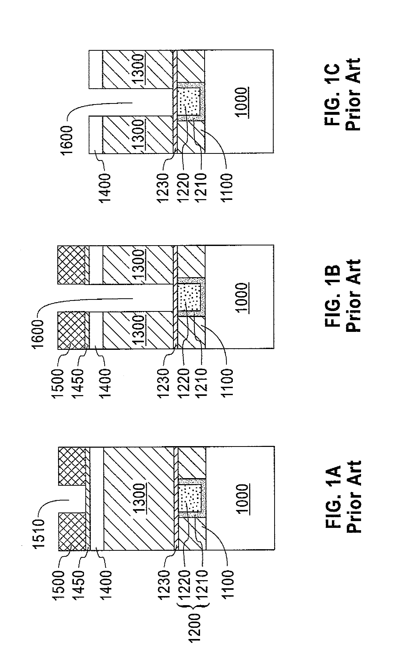
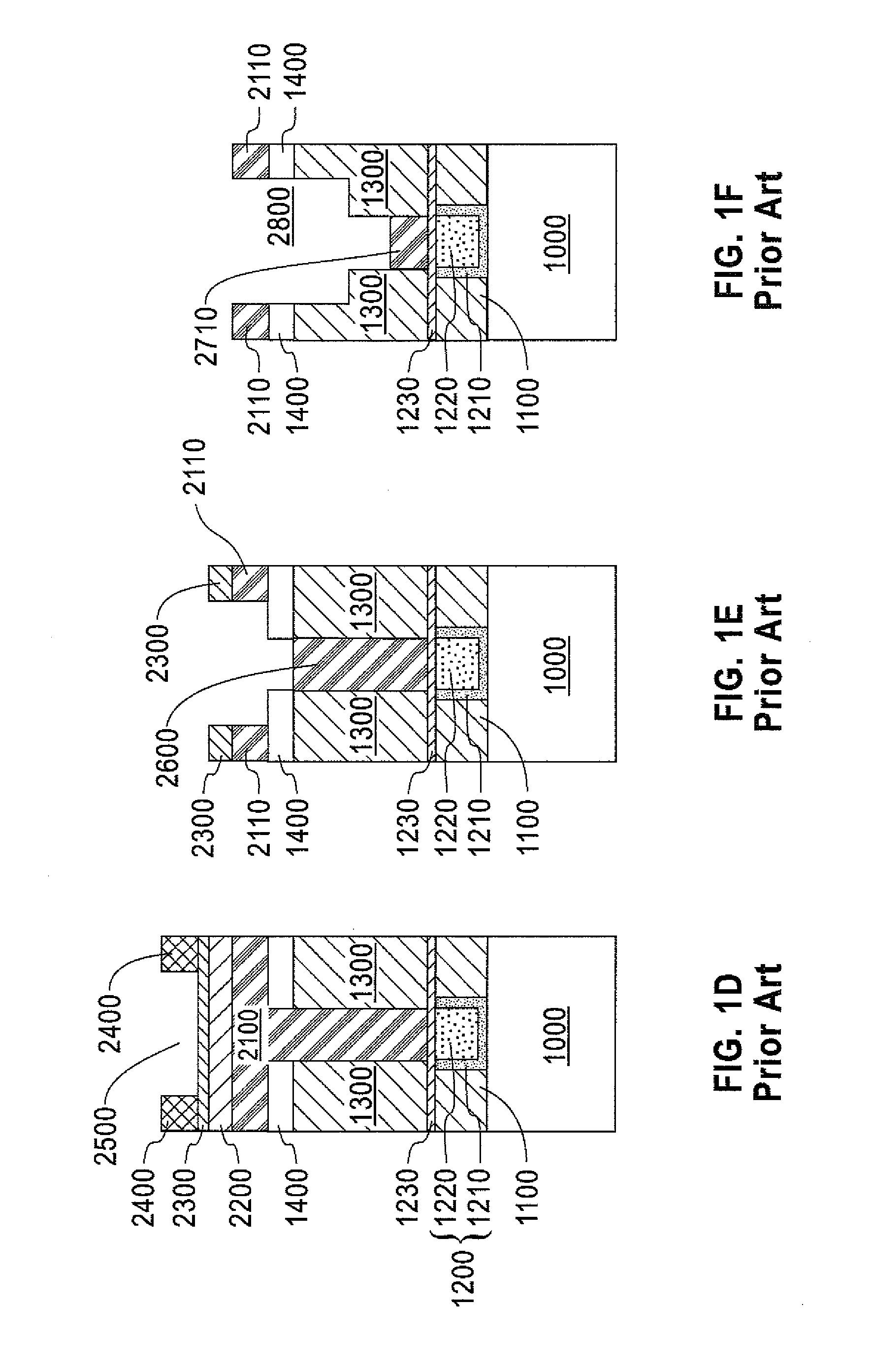
[0098]In embodiment 1, or the first embodiment, of the present invention, the integration sequence including the dual damascene etch and the plasma strip process described in FIGS. 1A-1I and accompanying paragraphs is interrupted after the patterning of the line trench 2800 in the second intermetal dielectric (IMD) layer 1300 and prior to removal of the patterned disposable material layer 2110 and the disposable via fill plug 2710. In other words, the prior art dual damascene process sequence described in FIGS. 1A-1F and accompanying paragraphs above are employed. For the sake of clarity, the prior art metal interconnect structure of FIG. 1F is reproduced as FIG. 2A with the same reference numerals. Thus, the first exemplary metal interconnect structure according to the first embodiment of the present invention shown in FIG. 2A is substantially the same as the prior art structure of FIG. 1F, and may be derived by the same processing steps known in the art.

[0...

embodiment 2

Use of a Sacrificial Layer

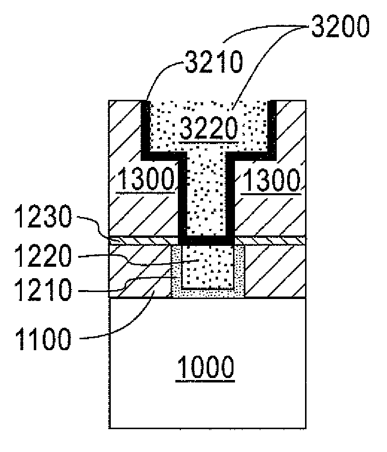
[0130]In embodiment 2, or the second embodiment, of the present invention, the integration sequence including the dual damascene etch and the plasma strip process described in FIGS. 1A-1I and accompanying paragraphs is interrupted after the patterning of the line trench 2800 in the second intermetal dielectric (IMD) layer 1300 and prior to removal of the patterned disposable material layer 2110 and the disposable via fill plug 2710 as in the first embodiment. For the sake of clarity, the prior art metal interconnect structure of FIG. 1F is reproduced as FIG. 3A with the same reference numerals. Thus, the second exemplary metal interconnect structure according to the second embodiment of the present invention shown in FIG. 3A is substantially the same as the prior art structure of FIG. 1F, and may be derived by the same processing steps known in the art.

[0131]Optionally, a short and mild plasma strip process or a mild wet clean that does not substantially al...

example 1

ILLUSTRATIVE EXAMPLE 1

Embodiment 1

[0141]A batch of 300 mm diameter silicon wafers was precleaned and coated with a 50 nm thick Si(CN) dielectric barrier film using a plasma enhanced CVD process known in the art. Next, a layer of a precursor film containing an organosilicate backbone and a pore forming labile organic agent (termed porogen) was deposited employing a process disclosed in one of U.S. Pat. Nos. 6,312,793; 6,437,443; and 6,479,110 to Grill et al., which are incorporated herein by reference.

[0142]The deposited film was then subjected to ultraviolet irradiation at 400° C. for a time period between 5 to 15 minutes to remove the labile porogen from the film and to enable good network crosslinking leading to an organosilicate film with a controlled volume fraction of pores with median diameter nominally less than 2 nm to form an ultra low k intermetal dielectric film. The k value of the ultra low k intermetal dielectric films is tunable and k values between 2.2 and 2.4 were ac...


PUM


Abstract

Methods of minimizing or eliminating plasma damage to low k and ultra low k organosilicate intermetal dielectric layers are provided. The reduction of the plasma damage is effected by interrupting the etch and strip process flow at a suitable point to add an inventive treatment which protects the intermetal dielectric layer from plasma damage during the plasma strip process. Reduction or elimination of a plasma damaged region in this manner also enables reduction of the line bias between a line pattern in a photoresist and a metal line formed therefrom, and changes in the line width of the line trench due to a wet clean after the reactive ion etch employed for formation of the line trench and a via cavity. The reduced line bias has a beneficial effect on electrical yields of a metal interconnect structure.

Description

RELATED APPLICATIONS[0001]The present application is related to a co-pending U.S. patent application Ser. No. ______ (Attorney Docket No. YOR920070333US1 (SSMP 21289)), which is incorporated herein by reference.FIELD OF THE INVENTION[0002]The present invention generally relates to methods of manufacturing a semiconductor structure, and particularly, to methods of manufacturing an interconnect structure having reduced signal propagation delay in a semiconductor circuit by minimizing plasma damage to low k and ultra low k organosilicate intermetal dielectric layers with a protective sidewall spacer.BACKGROUND OF THE INVENTION[0003]Advanced semiconductor chips, such as high performance microprocessor, microcontroller and communication chips, require high speed interconnect structures between individual semiconductor devices which are used to perform various functions such as logical operations, storing and retrieving data, providing control signals and the like. With the progress in th...

Claims


Application Information

Patent Timeline
Patent Type & Authority Applications(United States)
IPC IPC(8): H01L21/4763
CPCH01L21/02063H01L21/02126H01L21/02203H01L21/02274H01L21/02304H01L21/02348H01L21/76831H01L21/31138H01L21/31144H01L21/31633H01L21/76808H01L21/76814H01L21/76826H01L21/02362H01L2221/1063
Inventor ARNOLD, JOHN C.BONILLA, GRISELDACOTE, WILLIAM J.DUBOIS, GERAUDEDELSTEIN, DANIEL C.GRILL, ALFREDHUANG, ELBERTMILLER, ROBERT D.NITTA, SATYA V.PURUSHOTHAMAN, SAMPATHRYAN, E. TODDSANKARAPANDIAN, MUTHUMANICKAMSPOONER, TERRY A.VOLKSEN, WILLI
Owner ADVANCED MICRO DEVICES INC
Why Eureka
Try Eureka