
Organic semiconductor composite, organic transistor material and organic field effect transistor

a technology of organic transistors and organic semiconductors, applied in the direction of non-metal conductors, conductors, nanoinformatics, etc., can solve the problems of difficult to realize the reduction of production costs or the enlargement of the area of inorganic semiconductors, difficult to reduce costs, and limited materials capable of being used as substrates. , to achieve the effect of high charge mobility and high on/off ratio

Inactive Publication Date: 2010-04-29
TORAY IND INC
View PDF5 Cites 21 Cited by
  • Summary
  • Abstract
  • Description
  • Claims
  • Application Information

AI Technical Summary

Benefits of technology

[0008]It is the object of the present invention to provide an organic semiconductor composite which can be formed into a film by a coating process such as an inkjet process, has high charge mobility and can maintain a high on / off ratio even in air, an organic transistor material and an organic field effect transistor.Means for Solving the Problems
[0019]In accordance with the present invention, it is possible to provide an organic semiconductor composite which can be formed into a film by a coating process such as an inkjet process, has high charge mobility and can maintain a high on / off ratio even in air, an organic transistor material and an organic field effect transistor.

Problems solved by technology

However, it is difficult to realize the reduction in production cost or the enlargement of area in the inorganic semiconductor due to the constraints of manufacturing facilities.
Further, since the process for forming a film of inorganic semiconductor such as silicon is operated at extremely high temperature, there has been a problem that the variety of materials capable of being used as a substrate are limited.
However, for the low molecular organic semiconductors, a vacuum process such as vapor deposition is often employed and therefore there has been a problem that it is difficult to enlarge the substrate size and reduce in costs.
However, in conjugated polymers typified by poly(p-phenylene vinylene), it is difficult to obtain high orientation and adequate mobility has not been achieved.
However, there has been a problem that most of the polythiophenes are oxidatively doped with ambient oxygen to cause the increase in off-current and the decrease in on / off ratio.
However, in the FET devices using these materials, adequate mobility has not been achieved.
Further, as a technique for enhancing the mobility, a method of using a composite in which carbon nanotubes are dispersed in a film of an polymer organic semiconductor such as polythiophenes (for example, Patent Document 3), and a method of using a solid composition in which carbon nanorods or nanotubes are dispersed in organic semiconductor molecules (for example, Patent Document 4) are disclosed, but in all these methods, adequate mobility has not been achieved.

Method used

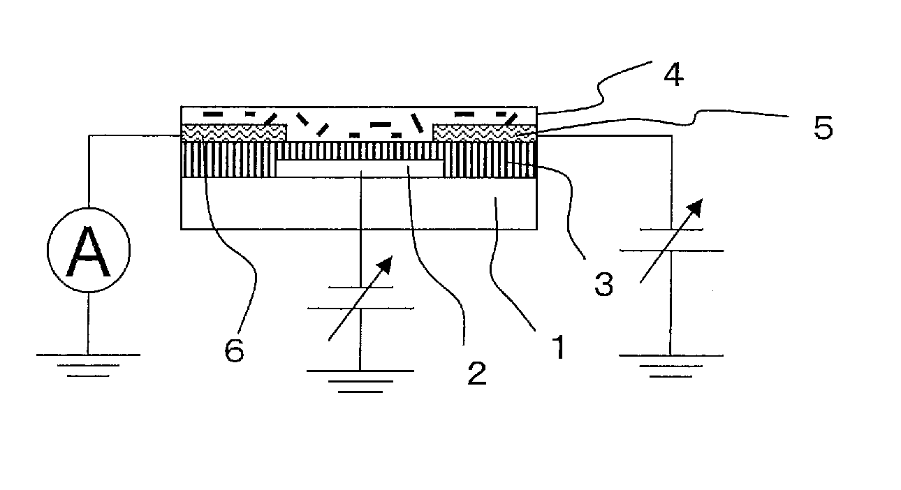
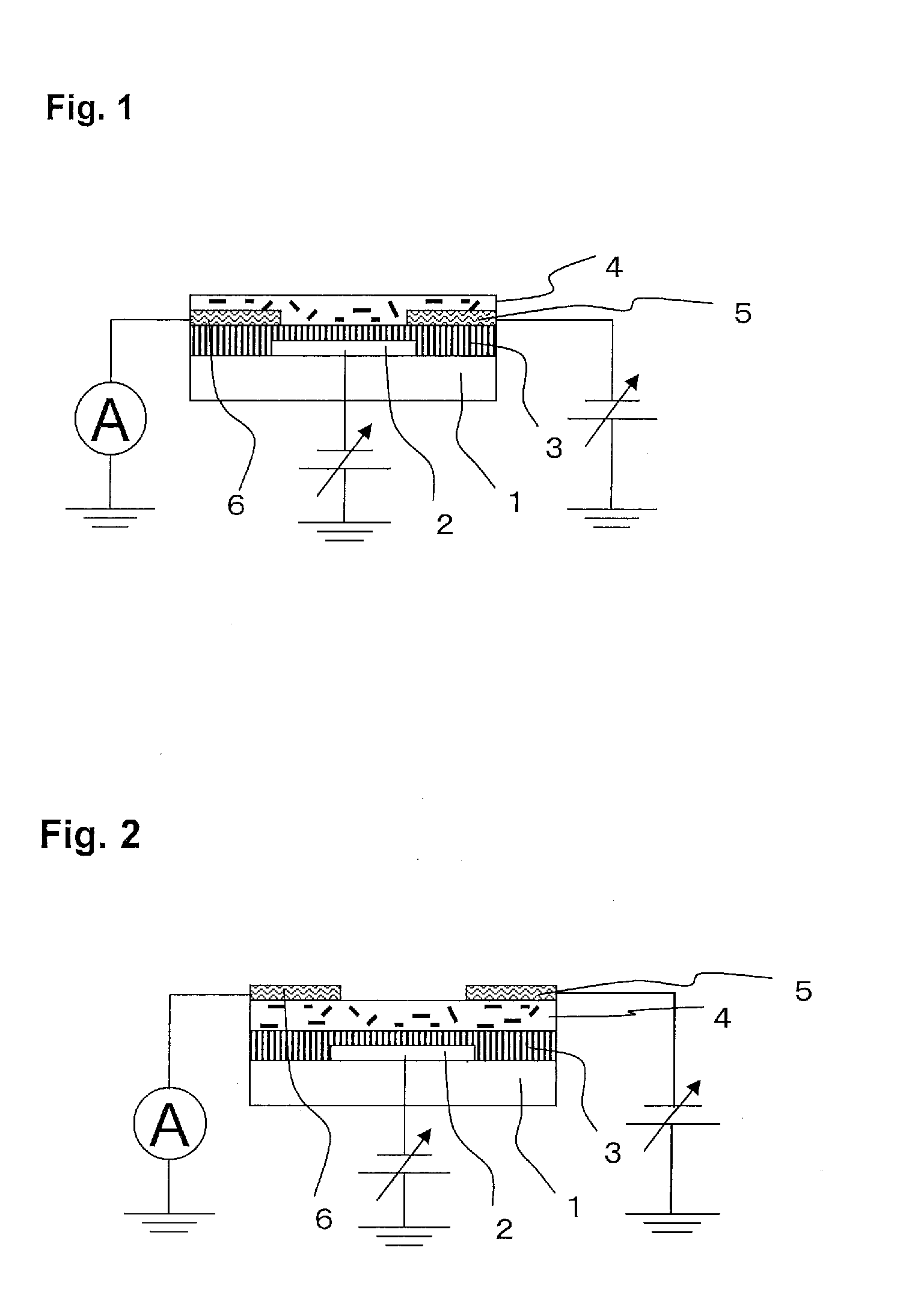

Image

  • Organic semiconductor composite, organic transistor material and organic field effect transistor
  • Organic semiconductor composite, organic transistor material and organic field effect transistor
  • Organic semiconductor composite, organic transistor material and organic field effect transistor

Examples


synthesis example 1

Synthesis of Compound [7]

[0130]60 g of 3-n-hexylthiophene was dissolved in 400 ml of dimethylformamide, and to this, 50 g of N-bromosuccinimide was added. The resulting solution was stirred at room temperature for 4 hours under a nitrogen atmosphere. 200 ml of water and 200 ml of hexane were added to the resulting solution to separate the organic layer. The organic layer was washed with 200 ml of water and dried over magnesium sulfate, and then the solvent was distilled off under reduced pressure with a rotary evaporator to obtain 60 g of 2-bromo-3-n-hexylthiophene.

[0131]Next, 4.3 g of magnesium powder and 10 mg of iodine were added to 100 ml of tetrahydrofuran and stirred for 30 minutes under a nitrogen atmosphere. To this, a mixture of 42 g of 2-bromo-3-n-hexylthiophene described above and 100 ml of tetrahydrofuran was added dropwise, and heated to reflux for 1 hour. The mixture was cooled to room temperature and a mixture of 20 g of 5,5′-dibromo-2,2′-bithiophene and 200 ml of tet...

synthesis example 2

Synthesis of Compound [6]

[0136]After a mixture of 16.3 g of 4T described above and 20 ml of tetrahydrofuran was cooled to −30° C., 21 ml of n-butyllithium solution (1.6 mol / l hexane solution) was added dropwise, and stirred at room temperature for 1 hour. The resulting mixture was cooled to −10° C., and 5.7 g of 2-isoporopoxy-4,4,5,5-tetramethyl-[1,3,2]dioxaborolane was added thereto and stirred at room temperature, for 3 hours. 33 ml of a 1N aqueous solution of hydrochloric acid, 200 ml of water and 200 ml of dichloromethane were added to the resulting solution to separate the organic layer. The organic layer was washed with 100 ml of water and then dried over magnesium sulfate. The resulting solution was concentrated by a rotary evaporator and was purified by a column chromatography (filler: silica gel, eluent: hexane / dichloromethane) to obtain 11 g of 4T-BPin represented by the following formula.

[0137]7.2 ml of ethanol, 12 ml of a 2N aqueous solution of sodium carbonate and 30 mg...

synthesis example 3

Synthesis of Compound [34]

[0140]A mixture of 3.1 g of 4,4′-bis(chloromethyl)biphenyl and 8.6 ml of triethylphosphite was stirred at 150° C. for 5 hours. The mixture was cooled to room temperature, and 50 ml of dimethylsulfoxide and 2.8 g of potassium t-butoxide were added to the mixture and stirred at room temperature for 10 minutes. Subsequently, 4.9 g of 3-hexyl-2-thiophene aldehyde was added thereto and stirred at room temperature for 5 hours. 30 ml of ethanol was added to the resulting solution and the precipitate was filtered to obtain a solid. The obtained solid was washed with 20 ml of ethanol to obtain 2.8 g of TPV represented by the following formula.

[0141]1.78 g of N-bromosuccinimide was added to a mixture of 2.8 g of TPV described above and 30 ml of dimethylformamide, and stirred at room temperature for 10 hours under a nitrogen stream. The resulting solution was filtered and the precipitate was washed with 10 ml of dimethylformamide and 20 ml of methanol to obtain 1.4 g ...


PUM

PropertyMeasurementUnit
Semiconductor propertiesaaaaaaaaaa

Abstract

The present invention provides an organic semiconductor composite containing a certain thiophene compound and carbon nanotubes, which can be formed into a film by a coating process such as an inkjet process, has high charge mobility and can maintain a high on / off ratio even in air, an organic transistor material and an organic field effect transistor.

Description

TECHNICAL FIELD[0001]The present invention relates to an organic semiconductor composite containing a thiophene compound and carbon nanotubes, an organic transistor material containing a thiophene compound and an organic field effect transistor.BACKGROUND ART[0002]Conventional field effect transistor devices (hereinafter, referred to as FET devices) use inorganic semiconductors such as silicon or germanium and require several stages of processes requiring much production cost such as photolithography and vacuum vapor deposition for forming circuit patterns. In semiconductor industries employing such production processes, requests for the reduction in production cost or large-area production in display are increased. However, it is difficult to realize the reduction in production cost or the enlargement of area in the inorganic semiconductor due to the constraints of manufacturing facilities. Further, since the process for forming a film of inorganic semiconductor such as silicon is ...

Claims


Application Information

Patent Timeline
IPC IPC(8): H01L51/30H01B1/24
CPCB82Y10/00H01L51/0005H01L51/0566H01L51/0068H01L51/0545H01L51/0048H10K71/135H10K85/221H10K85/655H10K10/466H10K10/488H01L21/18H01L29/772H10K10/00
Inventor MURASE, SEIICHIROJO, YUKARITSUKAMOTO, JUNMATA, JUNJI
Owner TORAY IND INC
Learn More