Vanadium Oxide Thin Film Pattern and Method of Fabricating the Same

a technology of vanadium oxide and thin film pattern, which is applied in the direction of non-linear optics, instruments, transportation and packaging, etc., can solve the problems of difficult formation of large areas, serious impact on the desirable properties of vanadium oxide, and inability to coat on low-heat-resistance substrates, etc., to achieve the effect of easy coating

Inactive Publication Date: 2010-07-22
NAT INST OF ADVANCED IND SCI & TECH
View PDF4 Cites 21 Cited by
  • Summary
  • Abstract
  • Description
  • Claims
  • Application Information

AI Technical Summary

Benefits of technology

[0073](6) By using a deposition reaction from a liquid phase, vanadium oxide can be easily coated on particles, fibers and substrates with complex shapes.

Problems solved by technology

However, the desirable properties of vanadium oxide are seriously affected by etching during micropatterning of the thin film.
Problems of prior art with regard to vanadium oxides include the impossibility of coating on low-heat-resistance substrates, the difficulty of forming large areas, the difficulty of coating substrates with complex shapes, and the high equipment and manufacturing costs and the like.
However, the desirable properties of vanadium oxides are seriously affected by etching during micropatterning of the thin film.

Method used


Image

  • Vanadium Oxide Thin Film Pattern and Method of Fabricating the Same
  • Vanadium Oxide Thin Film Pattern and Method of Fabricating the Same
  • Vanadium Oxide Thin Film Pattern and Method of Fabricating the Same

Examples


example 1

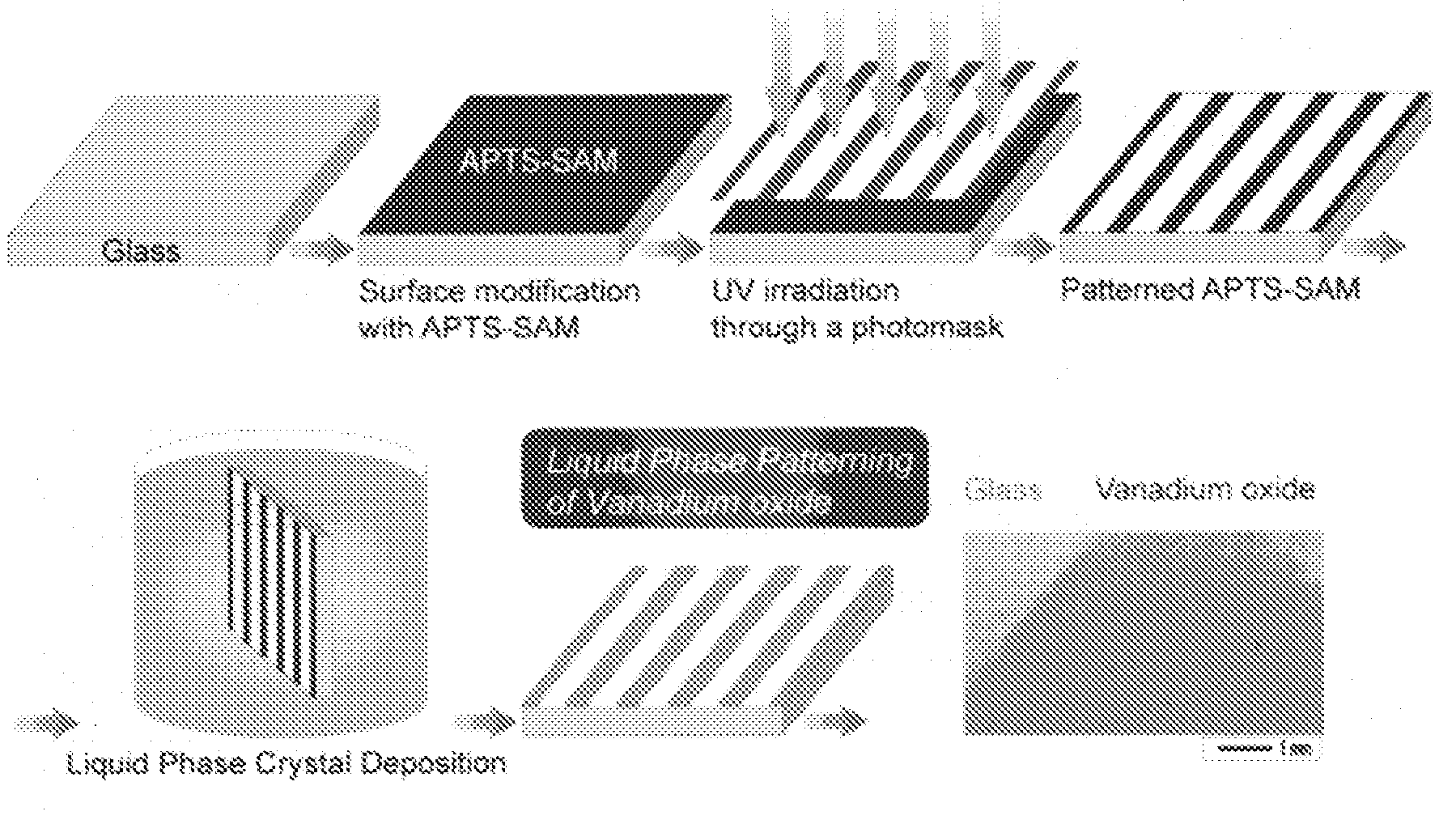
[0081]In this example, a vanadium oxide thin film pattern was prepared on a glass substrate using a self-assembled monolayer.

[0082](1) Preparation of Self-Assembled Monolayer

[0083]In this example, preparation of a vanadium oxide thin film was attempted using a self-assembled monolayer. A glass substrate (Hioki #1737, Corning Co.) was washed by ultrasound washing for 5 minutes each with acetone, ethanol and ion-exchange water in that order.

[0084]This was then irradiated for 10 minutes with vacuum ultraviolet using a UV ozone cleaner (184.9 nm and 253.7 nm, low-pressure mercury lamp 200 W, PL21-200, SEN Lights Co.) to remove adsorbed organic matter from the surface of the glass substrate.

[0085]Next, the glass substrate surface was modified with an APTS-SAM (surface modification with APTS-SAM). The APTS (3-aminopropyltriethoxysilane, H2NC3H5Si(OCH3)3) was dissolved to 1 vol % in anhydrous toluene, and the glass substrate was dipped for 2 hours in a nitrogen atmosphere in a glove box (V...

example 2

[0092](1) (Evaluation Methods)

[0093]In this example, the method in Example 1 described above is applied, and the zeta potentials of the particles produced in aqueous solution, the APTS self-assembled monolayer and the ATPS self-assembled monolayer after exposure to vacuum ultraviolet were measured with a laser zeta potentiometer (ELS-7300K, Otsuka Electronics Co., Ltd.).

[0094]The thin-film micropattern was observed with an optical microscope (BX51W1 Microscope, Olympus Optical Co., Ltd.) and an electron microscope (FE-SEM; JSM-6335F, JEOL Ltd.).

[0095]The crystal structure was evaluated with an X-ray diffraction meter (CuKα radiation XRD; RAD-1C, Rigaku). The transmissibility of the thin film at 25° C. and 70° C. was measured using a UV / VIS / NIR spectrophotometer (V-570, Jasco).

[0096]The samples in this case were fixed in an aluminum sample holder, and heated to 70° C. with an electrical heater fixed to the sample holder. The temperature of the thin film was measured with a thermocoup...

example 3

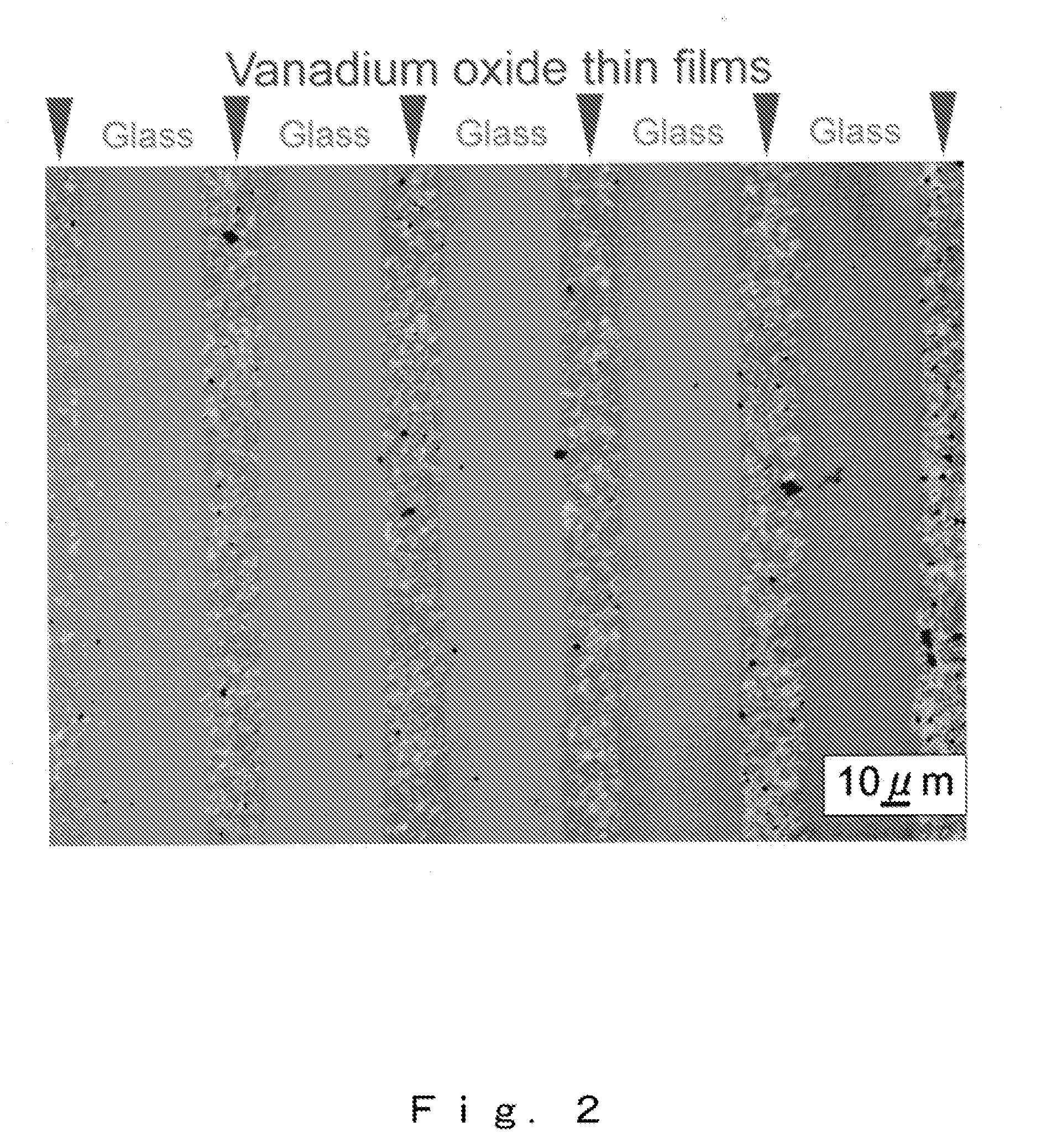
[0101](1) Morphology of Thin Film Surface

[0102]In this example, the detailed morphology of the surface of the thin film prepared in Example 1 above was observed by scanning electron microscopy. Before platinum coating, the sample exhibited a strong white color in the silanol group region in contrast with the amino group region, and this is attributed to strong electrical charging of the glass surface of the silanol region from electron beam irradiation. This indicates the difference in surface state between the glass and the vanadium oxide.

[0103]The patterned thin film was coated with 3 nm of platinum for an antistatic, and observed again. FIG. 3 shows an electron microscope image (3a) of the vanadium oxide images film pattern. (3b to 3d) of FIG. 3 show enlarged photographs of the vanadium oxide thin film surface. The amino group region appears somewhat whiter than the silanol group region, and this is attributed to thin film formation on the amino group region (FIG. 3a).

[0104]At hi...


PUM

PropertyMeasurementUnit
temperatureaaaaaaaaaa
boiling pointaaaaaaaaaa
pHaaaaaaaaaa

Abstract

The present invention relates to a vanadium oxide thin film pattern which is fabricated by using APTS (3-aminopropyltriethoxysilane, H2NC3H5Si(OCH3)3) or the like to prepare an APTS-SAM or the like on the surface of a substrate, irradiating this APTS-SAM with vacuum ultraviolet light through a photomask to thereby modify amino-terminal silanes into silanol groups in the exposed area, and then depositing vanadium oxide in a liquid phase using a patterned self-assembled monolayer having the amino-terminated silane surface and silanol group surface as a template for patterning the vanadium oxide, to a method of fabricating the same, and to a vanadium oxide device.

Description

TECHNICAL FIELD[0001]The present invention relates to a vanadium oxide thin film and vanadium oxide thin film pattern, and to a method of fabricating the same, and relates more particularly to a vanadium oxide thin film and vanadium oxide thin film pattern formed on the amino-terminated silane region of a self-assembled monolayer used as a template, to a method of fabricating the same, and to a device product thereof.[0002]The vanadium oxide thin film and vanadium oxide thin film pattern of the present invention is characterized by that has amino groups of an APTS-SAM, or N atoms derived from amino groups, at the boundary with the substrate. The present invention provides a vanadium oxide thin film and vanadium oxide thin film pattern, and a product thereof, that can be used preferably for thermoresponsive heat-shielding glass (smart windows), thermosensors and the like.BACKGROUND ART[0003]Vanadium oxides (VOx) have been highly paid attention to catalysts (Non-patent Document 1), el...

Claims


Application Information

Patent Timeline
Patent Type & Authority Applications(United States)
IPC IPC(8): B32B3/10B05D1/18B32B9/04
CPCB82Y30/00C01G31/02C01P2002/72C01P2002/82C01P2004/03C01P2004/04C01P2004/64C03C17/002C03C17/23C03C2217/218C23C26/00G02F1/0147G02F1/19Y10T428/31663Y10T428/24851Y10T428/24926Y10T428/24802
Inventor MASUDA, YOSHITAKEKOUMOTO, KUNIHITO
Owner NAT INST OF ADVANCED IND SCI & TECH
Why Eureka
Try Eureka