Semiconductor layer structure

a semiconductor layer and semiconductor technology, applied in the direction of semiconductor devices, lasers, semiconductor lasers, etc., can solve the problems of the ridge ld efficiency, the ratio of output optical power to input electrical energy, and the well known limits of the output power of the waveguide laser diode, so as to reduce the likelihood of defects and increase the electrical resistance

Inactive Publication Date: 2010-10-21
SHARP KK
View PDF3 Cites 29 Cited by
  • Summary
  • Abstract
  • Description
  • Claims
  • Application Information

AI Technical Summary

Benefits of technology

[0013]The present invention provides a III-nitride semiconductor multilayer structure, wherein a first layer of the structure comprises a layer of single crystal AlInN having a non-zero In content, the AlInN layer having at least one aperture whereby the AlInN layer does not extend over the area of the multilayer structure. It has been found that a high-resistance layer of AlInN may be used as a current confinement layer in a multilayer structure in the III-nitride material system. The aperture(s) correspond to the desired regions of current flow through the structure. This avoids the need to oxidise an AlInN layer in order to increase its electrical resistance, and avoids the disadvantages mentioned above. Moreover, the AlInN layer may be lattice-matched, or substantially lattice-matched (for example have a lattice mismatch of less than 1% or even of less than 0.5%) to an underlying layer in the multilayer structure, thereby reducing the likelihood of defects occurring in the multilayer structure.

Problems solved by technology

However conventional ridge-waveguide laser diodes exhibit some well know limits to how much output power can be obtained from these devices.
Indeed the wall plug efficiency (that is, the ratio of the output optical power to the input electrical energy) of a ridge LD tends to decrease for high current operating conditions.
This is related to the decrease of the maximum output power due to thermal rollover and high resistance in the device.
There have been difficulties in providing an effective current confinement layer in a light-emitting device fabricated in the (Al,Ga,In)N material system.
One disadvantage is that inactivation of carriers in BInAlGaN requires the use of a post-growth processing.
With this method, however, it can be difficult to precisely control the amount of impurities and the actual depth of layer compensated by this process.
Use of a layer with poor current blocking properties as a current blocking layer in an LD would create carrier leakage when the LD is in operation and degrade the performance.
As a result, a high dislocation density is present in a subsequent semiconductor layer formed on this re-crystallised AlN layer which can be the cause of device performance degradation.
If this method were used to make a current confinement layer in a laser diode device the formed oxide may cause reliability problems.
Also, the thermal conductivity of the oxide is often low which could also increase device degradation and the oxide layer might create additional lattice strain to the semiconductor structure leading also to device degradation.
Uniformity control of oxidation process is also known as an issue.
The oxidation depth in each mesa can often vary, owing to non-uniformity of the mesas dimension, layer thickness, position of the wafer in the solution, etc.
This results in current apertures with different dimensions over the wafer leading to poor manufacturing yield.
However the crystal quality of this layer is poor and exhibits some degree of crystalline mosaicity.
Use of this layer in a light emitting device would be expected to introduce defects in the structure because of the poor crystal quality of the layer.

Method used


Image

  • Semiconductor layer structure
  • Semiconductor layer structure
  • Semiconductor layer structure

Examples


first embodiment

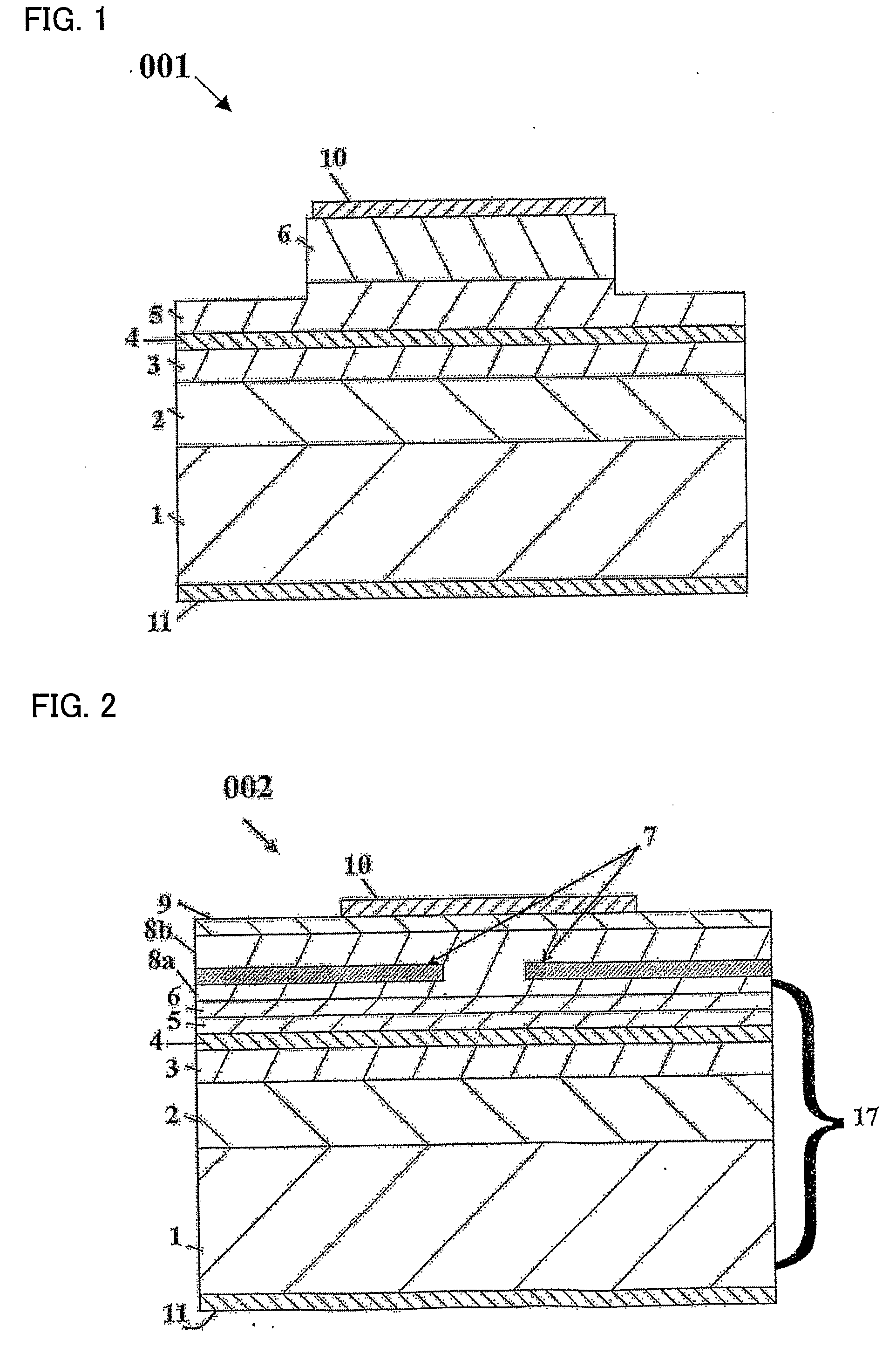
[0043]FIG. 2 shows a cross-sectional structure of a semiconductor laser 002 according to a first embodiment of the invention. The semiconductor laser 002 is also defined here as p-SAS. The semiconductor laser 002 includes a substrate, in this example a n-type GaN semiconductor substrate 1, and plurality of semiconductor layers which include a multilayer structure 17 having an active region for light-emission over the substrate. In the example of FIG. 2 the multilayer structure 17 includes a n-type AlGaN cladding layer 2, a n-type GaN guide layer 3, a multiple quantum well active region 4 containing In, a nominally undoped GaN guide layer 5, a p-type AlGaN carrier blocking layer 6, a p-type AlGaN cladding layer 8. The role of layer 6 is to prevent electron leakage from the active region. This layer is standard in nitrides semiconductor laser. A p-type GaN contact layer 9 is grown over the p-type AlGaN cladding layer 8. On the top surface of the contact layer 9 is a p-electrode 10 and...

second embodiment

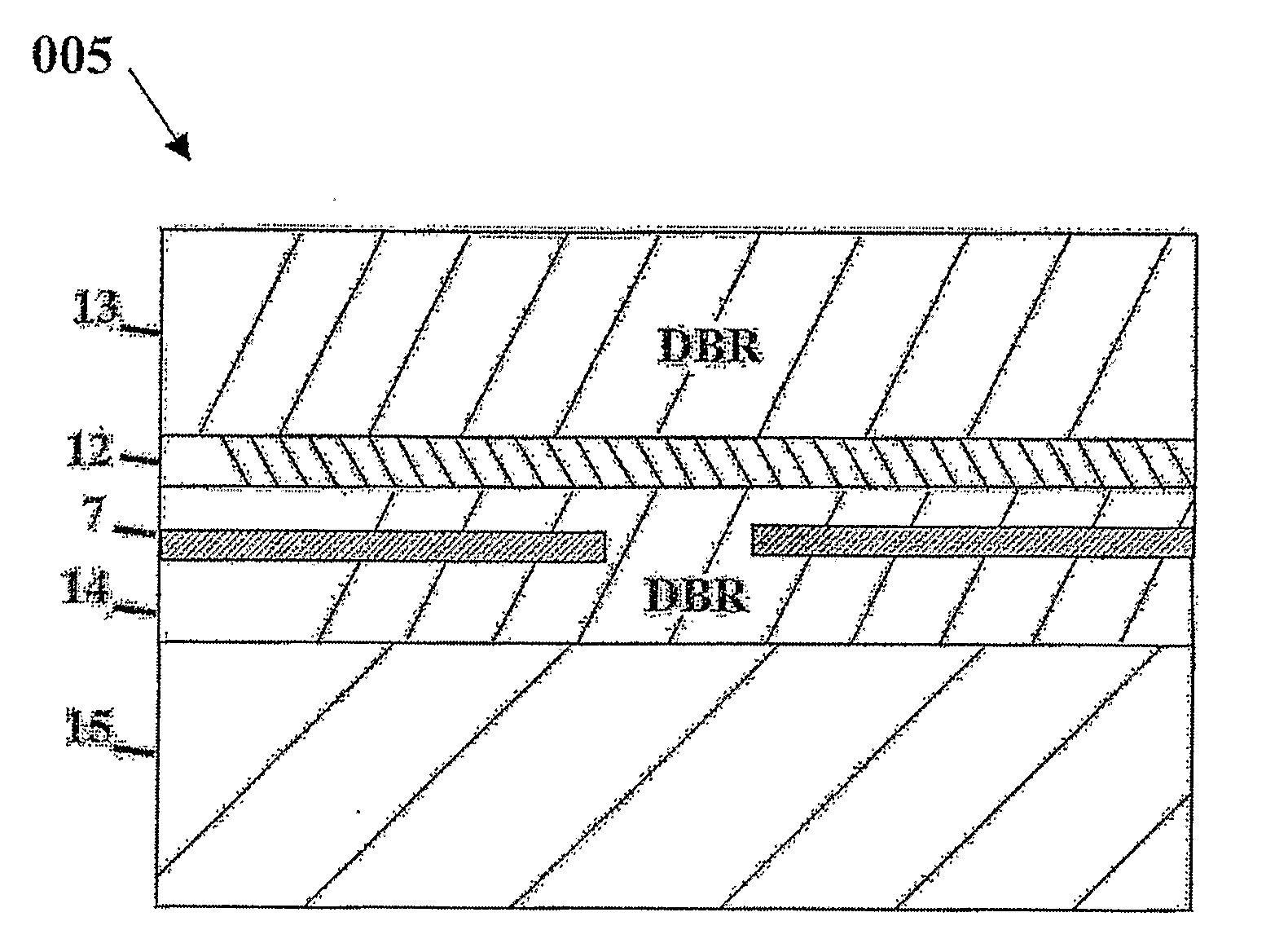
[0051]FIG. 5 shows a cross-sectional structure of a semiconductor laser diode 003 as a second embodiment of this invention. This semiconductor laser 003 is also called an n-SAS (self-aligned structure) laser diode. The semiconductor laser 003 includes a substrate, in this example a n-type GaN semiconductor substrate 1, and a multilayer structure including an active region for light-emission over the substrate. A current confinement layer 7 is provided in this multilayer structure. The second embodiment differs from the first embodiment in that, while the current confinement layer 7 is formed on the top surface of the p-AlGaN carrier blocking layer 6 in the first embodiment, the current confinement layer 7 is placed on the top surface of the n-type cladding layer 2 in the second embodiment.

[0052]The AlInN current confinement layer 7 is formed on the top surface of the n-type AlGaN cladding layer 2. The n-type GaN guide layer 3 is in contact with the top surface of the layer 7 and wit...

third embodiment

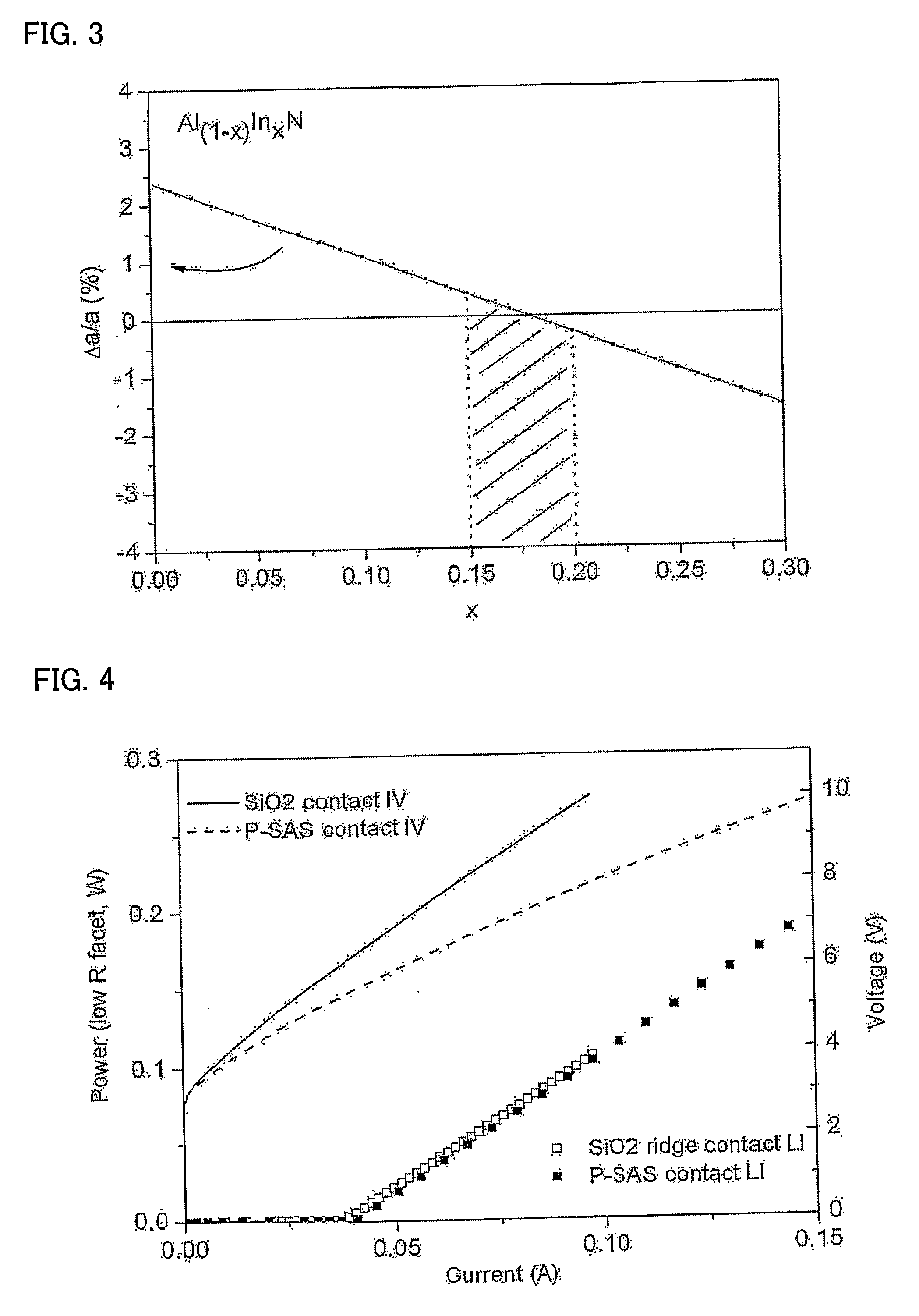
[0054]This third embodiment is a method of forming a resistive AlInN layer with high crystal quality on a surface of (Al,Ga,In)N nitride semiconductor. First a semiconductor substrate with a top surface of an (Al,Ga,In)N nitride semiconductor is placed in an MBE deposition chamber (step 1 of FIG. 16). Then the substrate temperature is raised to a suitable growth temperature (step 2 of FIG. 16). For growth of AlInN, a substrate temperature of between 550degC and 650degC would be suitable. Activated nitrogen is then supplied to the substrate surface by the mean of a RF plasma cell (step 3 of FIG. 16). Then the growth is started by supplying aluminium and indium to the growth chamber (step of FIG. 16). This makes possible the growth of a crystalline AlInN layer having high crystal quality.

[0055]Journal of Applied Physics Vol. 82, p 5472 (1997) presents an overview of the growth conditions used in PA-MBE for the growth of GaN. It is now accepted and demonstrated that, in order to obtain...


PUM


Abstract

A III-nitride compound device which has a layer of AlInN (7) having a non-zero In content, for example acting as a current blocking layer, is described. The layer of AlInN (7) has at least aperture defined therein. The layer of AlInN (7) is grown with a small lattice-mismatch with an underlying layer, for example an underlying GaN layer, thus preventing added crystal strain in the device. By using optimised growth conditions the resistivity of the AlInN is made higher than 102 ohm·cm thus preventing current flow when used as a current blocking layer in a multilayer semiconductor device with layers having smaller resistivity. As a consequence, when the AlInN layer has an opening and is placed in a laser diode device, the resistance of the device is lower resulting in a device with better performance.

Description

TECHNICAL FIELD[0001]The present invention relates to a III-nitride semiconductor layer structure having at least one layer of single crystal Al1-xInxN. The Al1-xInxN layer may be, for example, a current blocking layer. The structure may be incorporated in, for example, a semiconductor light-emitting device.BACKGROUND ART[0002]In the last decade, gallium nitride (GaN) based semiconductor light-emitting devices have been of considerable interest in the field of optical storage. Today the demand for high power laser diodes (LD) and light emitting diodes (LED) is growing, for example for use in high performances optical disk systems and novel applications i.e. solid state lighting, display backlighting, etc.[0003]It is often desirable for a laser diode to have some means of providing lateral confinement of current flowing through the laser diode, in order to provide lateral confinement of the generated light. For example in an LD it is common practice to employ a ridge-waveguide struct...

Claims


Application Information

Patent Timeline
Patent Type & Authority Applications(United States)
IPC IPC(8): H01S5/323H01L33/30H01L21/20
CPCH01L21/02389H01L21/0254H01L21/02631H01S5/32341H01S5/2216H01S5/2231H01S5/221H01L33/145H01L33/32
Inventor BOUSQUET, VALERIEKAUER, MATTHIASTAN, WEI-SINHEFFERNAN, JONATHANTAKAHASHI, KOJI
Owner SHARP KK
Why Eureka
Try Eureka