
Photonic crystal microarray device for label-free multiple analyte sensing, biosensing and diagnostic assay chips

a microarray and label-free technology, applied in the field of optical and medical devices, can solve the problems of large sensitivity to changes in the refractive index of the ambient, poor quality, and design that is not suitable for the fabrication of microarrays for multiple analyte sensing, and achieve the effect of increasing the measurement throughput of the device and enhancing sensitivity

Active Publication Date: 2011-02-03
OMEGA OPTICS
View PDF10 Cites 39 Cited by
  • Summary
  • Abstract
  • Description
  • Claims
  • Application Information

AI Technical Summary

Benefits of technology

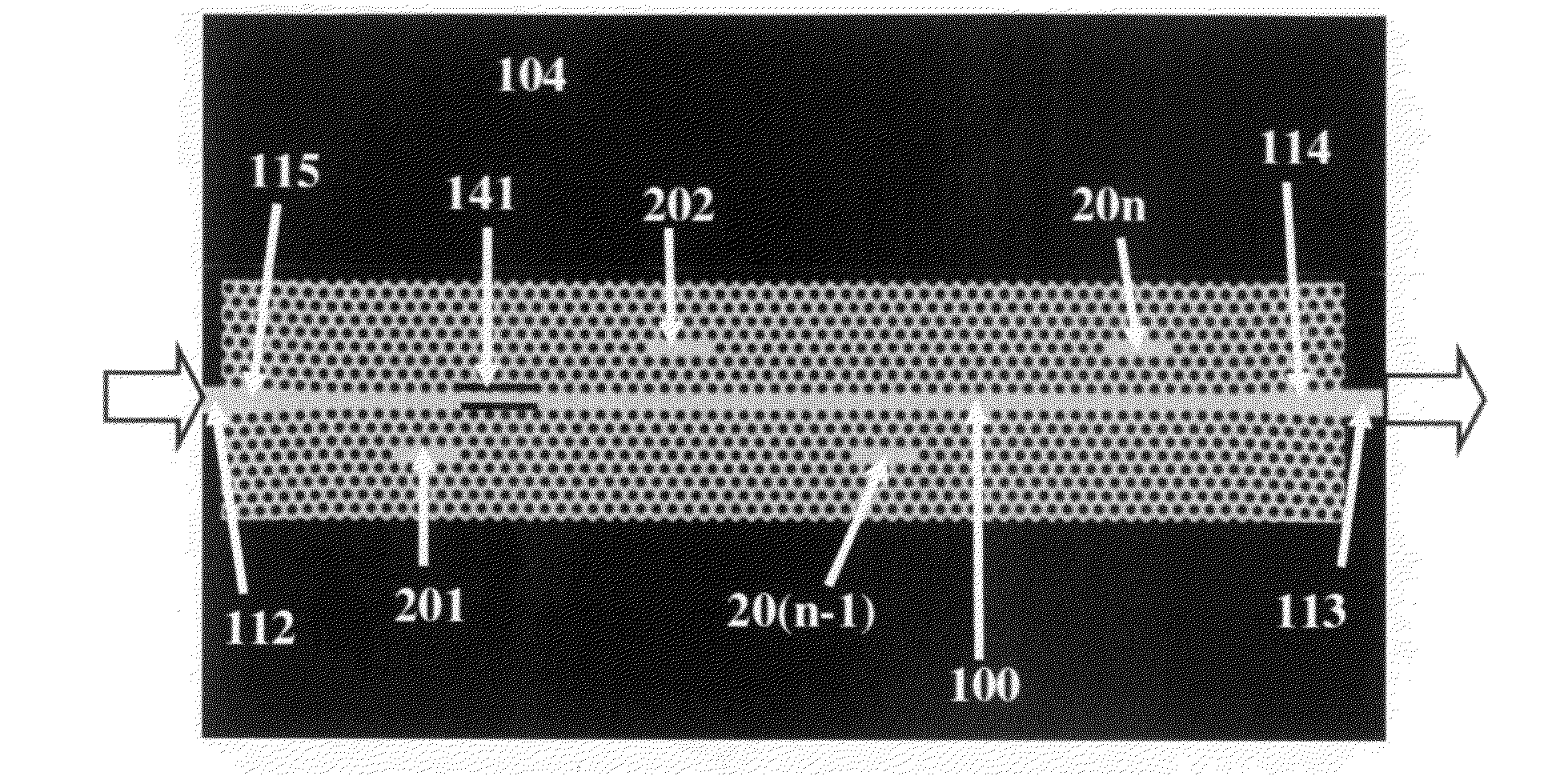
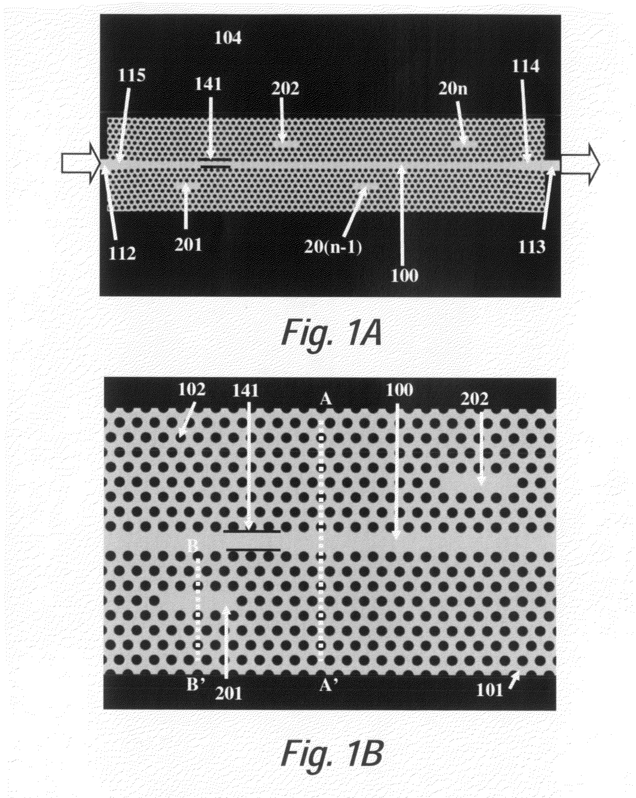
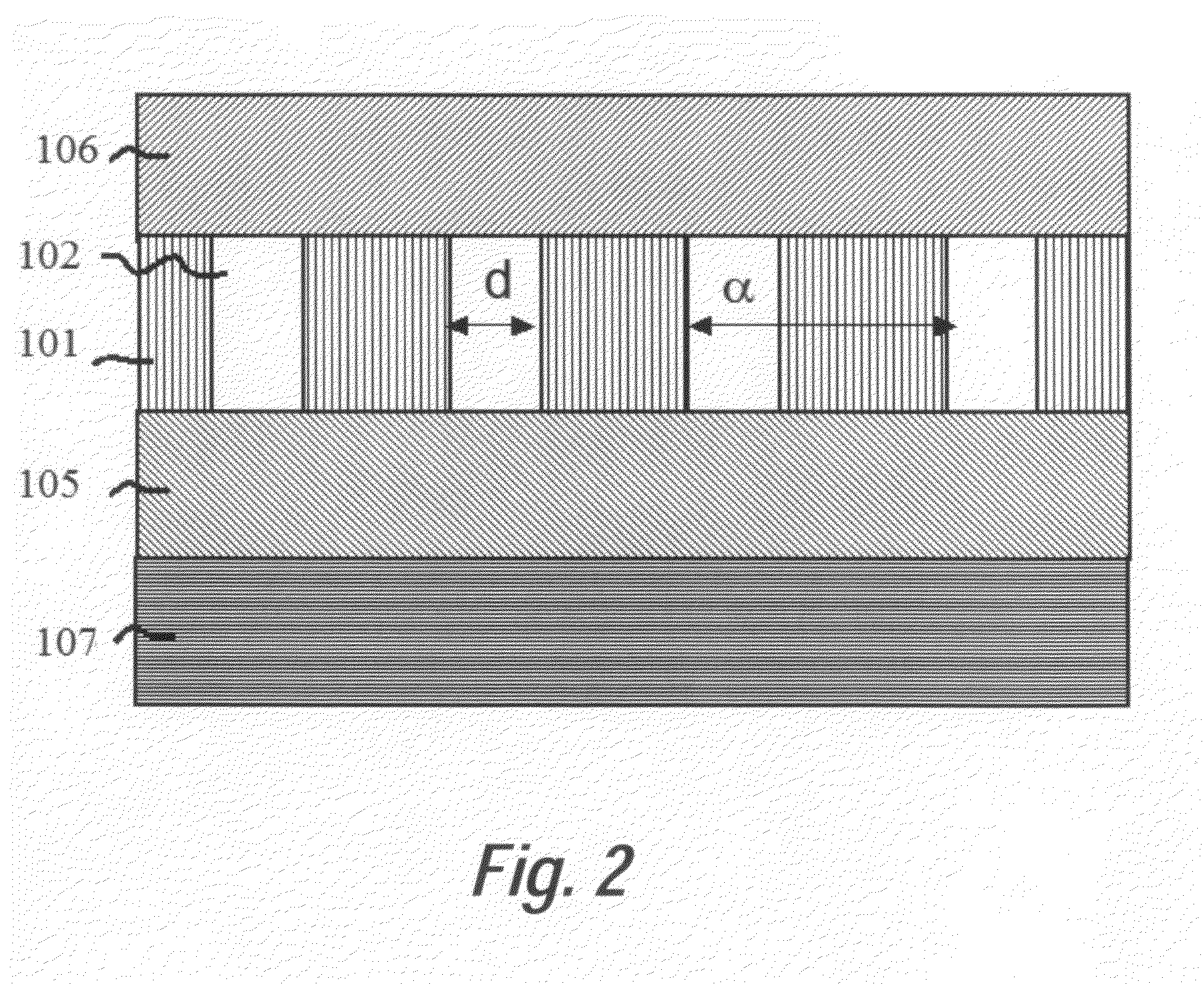
One embodiment of the invention provides a sensor comprising a semiconductor material core with high dielectric constant, supported on the bottom by a low dielectric constant cladding. A triangular lattice of photonic crystal holes is etched into the substrate. Photonic crystal waveguide is defined by filling a single row of holes, from input ridge waveguide transition to output ridge waveguide transition with the semiconductor core material. Photonic crystal microcavity is similarly defined by filing a few holes with semiconductor core material. Multiple photonic crystal microcavities are patterned at a distance of three lattice constants from the photonic crystal waveguide. The distance between individual photonic crystal microcavities is 10 lattice periods. The high dielectric constant core with structured photonic crystal waveguide and photonic crystal microcavities, together with the low dielectric constant cladding, form the photonic crystal microarray structure. Light is coupled into the photonic crystal waveguide from a ridge waveguide. Light is out-coupled from the photonic crystal waveguide to an output ridge waveguide. When a broadband light source is input to the photonic crystal waveguide, wavelengths corresponding to the resonant wavelengths of the individual microcavities are coupled to the corresponding microcavities. As a result, minima are observed in the transmission spectrum corresponding to the dropped wavelength of each photonic crystal microcavity. Depending upon the wavelength range of interrogation, the period of the sub-wavelength lattice can vary from 50 nm to 1500 nm and the depth of the lattice structure can vary from 0.4 to 0.7 times the lattice periodicity above. The semiconductor material can be silicon (or any Group IV material), gallium arsenide (or any III-V semiconductor) or any semiconductor material with high refractive index. The substrate can be any Group IV material corresponding to the Group IV core material, or any substrate suitable to grow the III-V core material. Above the microcavity, a thin film of target binding molecules that are immobilized on the microcavity surfaces, each microcavity surface being coated with an exclusive target molecule or biomolecule, forms the dielectric coating. The one or more binding molecules are free of detection labels. The one or more specific binding substances are thus arranged in an array on the microcavities, along the photonic crystal waveguide. A single transmission spectrum therefore probes the binding events on multiple microcavities. A binding event on a specific microcavity shifts the corresponding transmission minimum and leads to a sensing event for the specific microcavity. Analyzed biomolecules can be proteins, DNA, RNA, small molecules or genes. Arrays of microcavities therefore lead to a multiple analyte sensing device that increases the measurement throughput of the device, in addition to the obvious sensitivity enhancements achieved by using two-dimensional photonic crystal waveguide coupled to two-dimensional photonic crystal microcavities.
The second objective of the invention is to eliminate the need for labeling of biomolecule and biomolecule conjugates for on-chip detection and thereby reduce microarray costs associated with biomolecule labeling.
The third objective of the invention is to significantly increase measurement throughput from devices by signal collection and analysis from multiple elements of a microarray in a single measurement as opposed to individual element measurement in contemporary systems.
The fourth objective of the invention is to implement a novel lithography scheme on a CMOS chip that avoids high temperature processes associated with photolithography and chemical etching for the patterning of multiple biomolecules and thereby preserves biomolecule functionality in aqueous phase at room temperatures or even colder if necessary.

Problems solved by technology

Tight confinement of the optical field in photonic crystal microcavities leads to a strong interaction with the surrounding ambient in the vicinity of the microcavity, thereby leading to large sensitivity to changes in refractive index of the ambient.
One dimensional photonic crystal microcavities, in addition to poor optical confinement, do not utilize the slow light effect due to reduced group velocity in two-dimensional photonic crystal waveguides that would otherwise enhance coupling efficiency and thereby improve signal-to-noise ratio of sensing.
In either case, the design is not suitable for the fabrication of microarrays for multiple analyte sensing.
The design demonstrated by Guillermain et al (see Guillermain E, Fauchet P. M., “Multi-channel sensing with resonant microcavities coupled to a photonic crystal waveguide,” JWA 45, CLEO Conference (2009)) in effect employs multiple photonic crystal waveguides and also employs microcavities with significantly poor quality factors that make the designs unsuitable for high sensitivity sensing.
At the very least, temperatures this high compromise or alter biological functionality, and at the very worst they may destroy its function.

Method used


Image

  • Photonic crystal microarray device for label-free multiple analyte sensing, biosensing and diagnostic assay chips
  • Photonic crystal microarray device for label-free multiple analyte sensing, biosensing and diagnostic assay chips
  • Photonic crystal microarray device for label-free multiple analyte sensing, biosensing and diagnostic assay chips

Examples


Embodiment Construction

Detailed Description of the Invention

In accordance with a preferred embodiment of the present invention, a device for a microarray for personalized diagnostic applications comprises: a functional photonic crystal waveguide having a waveguide core along which light is guided, arrays of photonic crystal microcavities along the length of the photonic crystal waveguide each coated with a separate biomolecule specific to disease identification, an input and output photonic crystal waveguide with gradually changed group index before and after the functional photonic crystal waveguide, which can bridge the refractive indices difference between conventional optical waveguides and the functional photonic crystal waveguide. The sensor can be used to detect organic or inorganic substances such as proteins, DNA, RNA, small molecules, nucleic acids, virus, bacteria, cells, genes, without requiring labels such as fluorescence or radiometry. Light (from a broadband source or LED) coupled into a ph...


PUM


Abstract

Methods and systems for label-free multiple analyte sensing, biosensing and diagnostic assay chips consisting of an array of photonic crystal microcavities along a single photonic crystal waveguide are disclosed. The invention comprises an on-chip integrated microarray device that enables detection and identification of multiple species to be performed simultaneously using optical techniques leading to a high throughput device for chemical sensing, biosensing and medical diagnostics. Other embodiments are described and claimed.

Description

BACKGROUND OF THE INVENTION1. Field of the InventionThis invention relates generally to the field of optical and medical devices, and more specifically to an apparatus and method for microarray implementation for the detection of multiple analytes such as chemical agents and biological molecules using photonic crystals.2. Background of the InventionLabel-free optical sensors based on photonic crystals have been demonstrated as a highly sensitive potential method for performing a large range of biochemical and cell-based assays. For background information on photonic crystals, the reader is directed to Joannopoulos, J. D., R. D. Meade, and J. N. Winn, Photonic Crystals, 1995 Princeton, N.J.: Princeton University Press. Tight confinement of the optical field in photonic crystal microcavities leads to a strong interaction with the surrounding ambient in the vicinity of the microcavity, thereby leading to large sensitivity to changes in refractive index of the ambient. Much of the resea...

Claims


Application Information

Patent Timeline
IPC IPC(8): C40B30/10C40B60/12
CPCG01N33/54373G01N21/253
Inventor CHAKRAVARTY, SWAPNAJITCHEN, RAY T.
Owner OMEGA OPTICS
Learn More