Optical Sensor Unit for Evanescence Wave Spectroscopy

a technology of evanescence wave and optical sensor, which is applied in the direction of instruments, special surfaces, coatings, etc., can solve the problems of poor sensitivity toward small molecules, inability to meet the requirements of chemical and electrical stability, reproducibility, biochemical surface modification, and inability to bio-integration, etc., to achieve high transmission, high selectivity, and high sensitivity. sensitivity

Active Publication Date: 2011-04-21
ADAMANTIS AB
View PDF8 Cites 24 Cited by
  • Summary
  • Abstract
  • Description
  • Claims
  • Application Information

AI Technical Summary

Benefits of technology

[0013]Herein we describe various aspects and embodiments of the invention related to a method and device for analysis of chemical of biological substances, in particular using an infrared light waveguide made of nanocrystalline diamond (NCD) or coated with a thin layer of NCD on polycrystalline diamond. The materials, methods and light propagation geometry are chosen so that the combination yields high transmission, favorable analysis condition and versatile surface chemical functionalization properties to achieve high selectivity, sensitivity, and throughput analysis as well as easy-to-use and reproducible operation. According to one embodiment, the waveguide comprises NCD, preferably NCD with diamond-like properties, in particular NCD with diamond-like broad band transmission properties. The waveguide may either be comprised of pure NCD or a NCD film which is coated onto a high-refractive index infrared material, such as Ge, diamond, Si, silver halide, InGaSb, and chalcogenide, capable of narrow or broad band transmission of light, in particular infrared light. According to one embodiment, the NCD film is coated on intermediate layers with intermediate refractive index between the waveguide and the NCD film to ensure simultaneous efficient light coupling and beneficial bonding properties between the NCD film, underlying layers and waveguide materials, which ensures mechanical stability and avoids chemical mixing (diffusion) of elements between the films. According to one particular embodiment, the NCD film is coated directly onto diamond, preferably high grade IR optical quality diamond, and in particular high grade mid-IR optical quality diamond.
[0014]The waveguide may be a free-standing device or be supported on a substrate material which may contain additional films or cladding layers with low refractive index compared t...

Problems solved by technology

Current transducer materials like polystyrene beads, carbon electrodes, gold, silicon, oxidized silicon and glass do not meet the requirements of smoothness, homogeneity, chemical and electrical stability, reproducibility, and biochemical surface modifications, and are not amenable for bio-integration [1].
Drawbacks with current commercial techniques include poor sensitivity toward small molecules (SPR and QCM), and unspecific analyte binding.
Fluorescent techniques rely on changes of fluorescent properties, which work well for some molecules but not for others; otherwise tedious additions of fluorescent labels are requ...

Method used


Image

  • Optical Sensor Unit for Evanescence Wave Spectroscopy
  • Optical Sensor Unit for Evanescence Wave Spectroscopy
  • Optical Sensor Unit for Evanescence Wave Spectroscopy

Examples


example 1

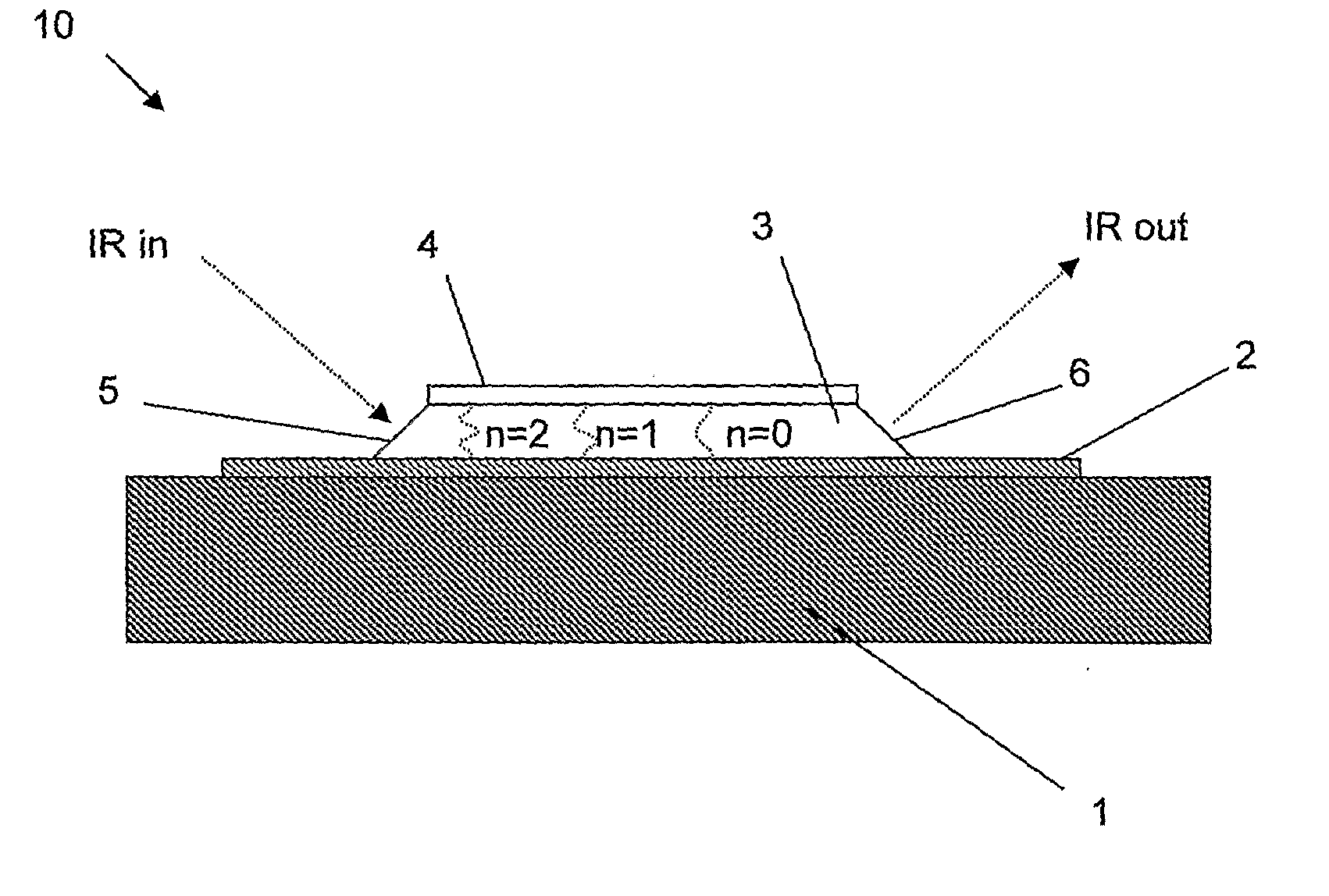
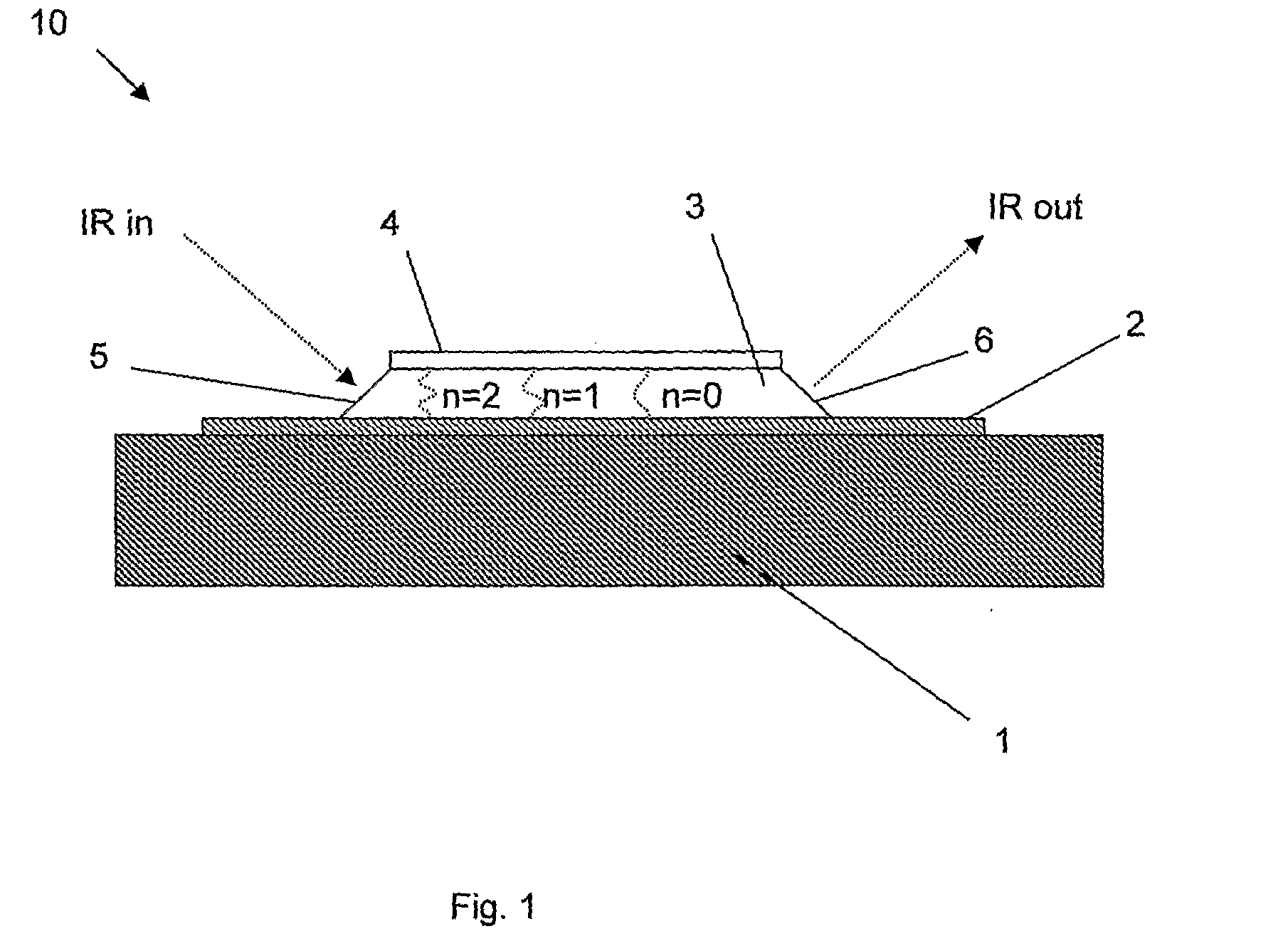
[0053] Nanocrystalline diamond films were grown by a hot-wire CVD method from a CH4 / H2 mixture [16]. The crystal size is in the nanometer range in agreement with our independent results from the Raman measurements presented above. Based on the optical characterization, NCD film growth limitations, our theoretical results, a final waveguide design included a 2 μm thick SiO2 layer grown by oxidation in wet atmosphere at 1050 degrees Celsius of the silicon substrate. The diamond waveguide was constructed from a 10 μm thick poly-crystalline diamond film of infrared optical quality grown ontop of the SiO2 / Si substrate with an additional thin (0.1 μm) NCD layer grown on the poly-crystalline diamond film. We use polycrystalline diamond as waveguide and grow NCD on top of the poly-crystalline film rather than having a thick NCD film. The reason for this is mainly because the poly-crystalline diamonds has in general superior optical properties and scatter less light than NCD films. With poly...

example 4

[0058 gives a theoretical description of a mid-IR diamond waveguide supported on a Si substrate with a thin SiO2 layer grown on top of the Si substrate. We use two different models to describe the waveguide device in FIG. 1: Mode analysis denoted Model 1) and Finite Element Method (FEM) denoted Model 2. The models are used to compute the transmission as a function of dimensions, wavelength and choice of materials. The refractive indices, n, used in the computations (both with Model 1 and Model 2) are as follows: n(Air)=1, n(Si)=3.4, SiO2)=1.46, and n(diamond)=n(NCD)=2.4. Tabulated experimental values of the optical constants for water (n and k) have been used to construct functions that describe their wavelength dependence. We have assumed that Si, SiO2 and the diamond materials are completely lossless (i.e., k=0) in the computations. Thus, intrinsic absorption in these materials is neglected in the computed results. We make no distinction of the optical properties of the diamond wa...


PUM


Abstract

Optical sensor unit for infra red evanescence wave spectroscopy (IR-EWS) analysis of chemical and biological substances in an analyte, comprising a waveguide with a sensor surface to be put into contact with the analyte, wherein the sensor surface is provided with an affinity enhancing layer. There is further provided a method of producing an optical sensor unit.

Description

[0001]The present invention relates to the art of evanescence wave spectroscopy analysis of chemical and biological substances in an analyte, and in particular to an optical sensor unit for evanescence wave spectroscopy.BACKGROUND TO THE INVENTION[0002]There is a huge demand of new types of sensor surfaces and devices that can readily be functionalized for sensitive, selective and quantitative analysis of broad spectrum chemical and biological substances. It is desirable to study real-time molecular interactions, preferable in situ or even in vivo. This is important not only since this opens up the possibility for immediate signal read-out (high throughput), but also because it gives additional information of the kinetics and discrimination of multiple molecular binding. At the same time these sensor surfaces and devices should be suitable for repeated usage (mechanical and chemical stable), function in a wide range of environmental conditions (pH, temperature, pressure, and chemica...

Claims


Application Information

Patent Timeline
IPC IPC(8): G01N21/35B05D5/06
CPCG01N21/552G01N21/7703G01N21/3577G02B2006/12035G02B6/102
Inventor OSTERLUND, LARSANDERSSON, PER OLAKARLSSON, MIKAELNIKOLAJEFF, FREDRIK
Owner ADAMANTIS AB
Why Eureka
Try Eureka