
Dye solar cell with improved stability

Active Publication Date: 2012-01-26
BASF SE
View PDF6 Cites 24 Cited by
  • Summary
  • Abstract
  • Description
  • Claims
  • Application Information

AI Technical Summary

Benefits of technology

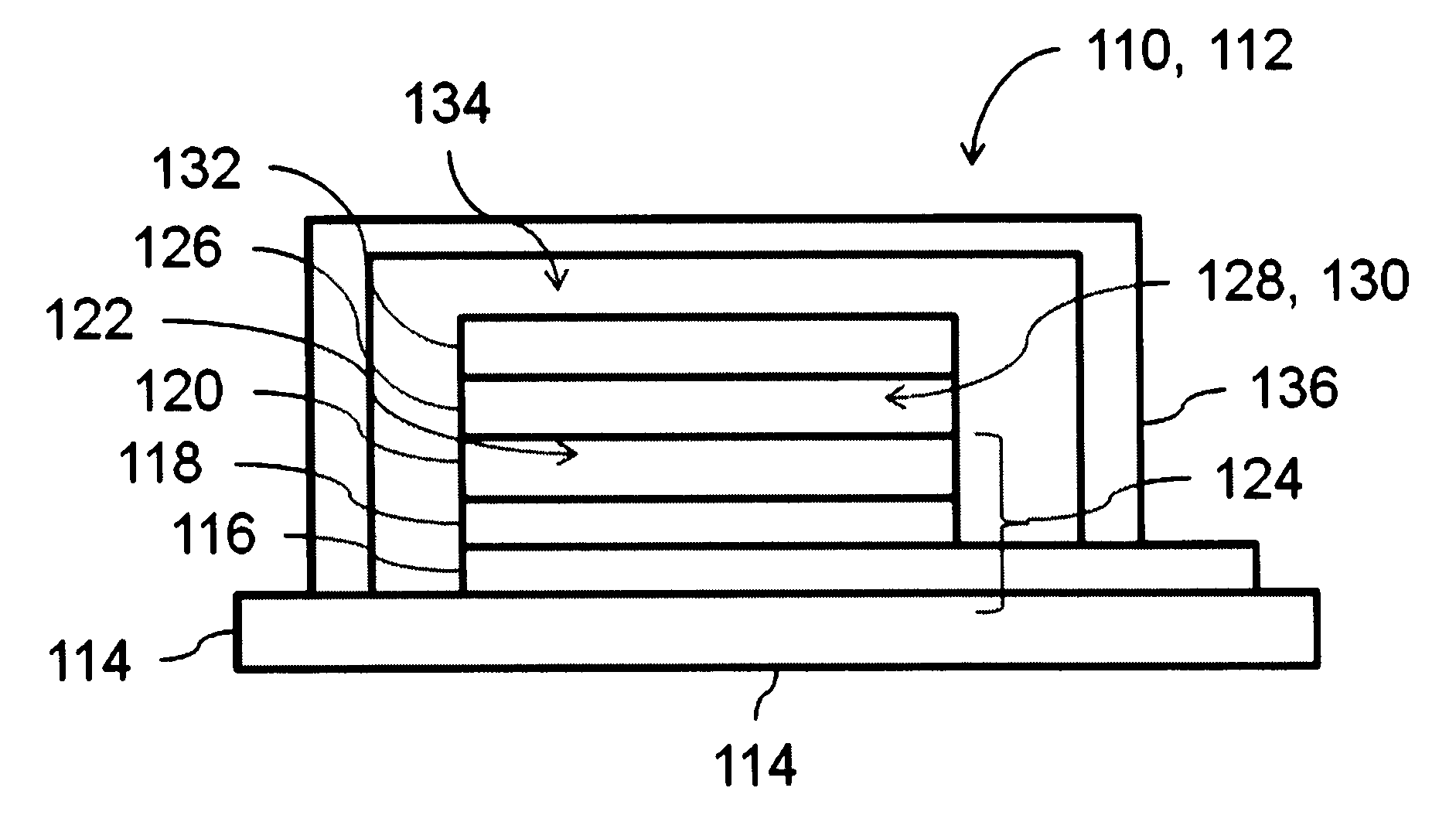
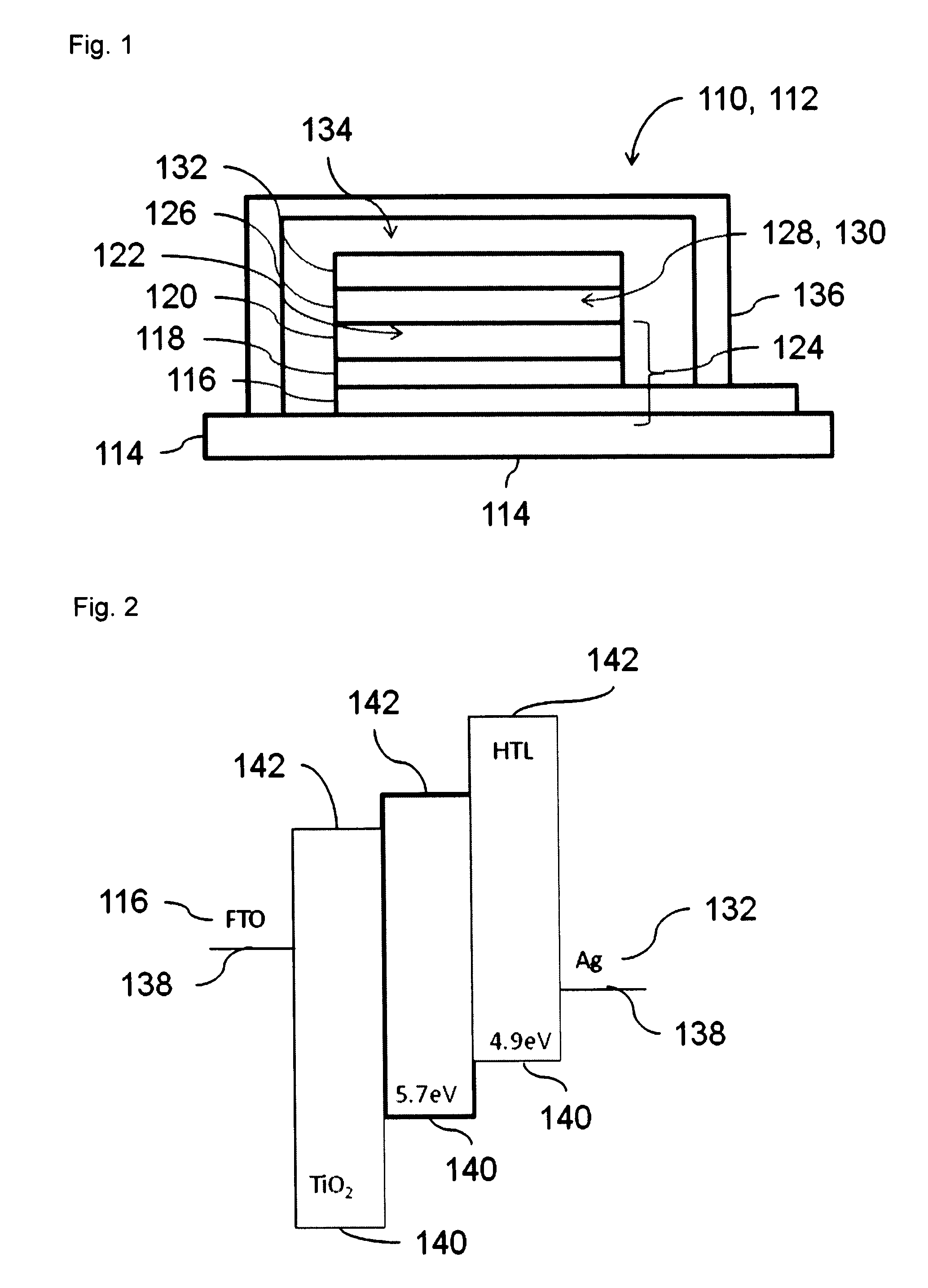
[0070]As a particular advantage of the present invention, the photovoltaic element may especially comprise at least one encapsulation. In contrast to conventional photovoltaic elements, in which solid p-semiconductors are doped by means of oxygen (for example by storage under air), the p-semiconductors doped with the at least one metal oxide may also exist without such an oxygen atmosphere over a prolonged period. Accordingly, it is possible to apply an encapsulation which screens the photovoltaic element, especially the electrodes and / or the p-semiconductor, from a surrounding atmosphere. In this way, in spite of the improvement in properties of the p-semiconductor by virtue of the doping by means of the metal oxide, oxygen can be excluded, which protects, for example, one or more of the electrodes from adverse effects resulting from oxygen and / or other surrounding gases. For example, the electrode degradation can be prevented in this way. The encapsulation may, for example, comprise encapsulation by a solid capsule element, for example a plane or capsule equipped with at least one depression, which is applied to the layer structure, for example, in such a way that it completely or partially surrounds the layer structure. For example, an edge of the encapsulation may completely or partially surround the layer structure and, for example, may be bonded to the substrate by an adhesive bond and / or another bond, preferably a cohesive bond. Alternatively or additionally, the encapsulation may also comprise one or more layers of a material which prevents penetration of harmful environmental influences, for example moisture and / or oxygen. For example, organic and / or inorganic coatings can be applied to the layer structure. Screening from ambient atmosphere can generally be understood to mean slowing of the penetration of gases and / or moisture from the surrounding atmosphere into the layer structure. The slowing can be effected, for example, in such a way that concentration differences within and outside the encapsulation are balanced out only within several hours, preferably several days, especially even several weeks, months extending up to years.
[0071]The dye solar cell may additionally have, between the n-semiconductive metal oxide and the p-semiconductor, especially at least one passivation material. The passivation material may especially serve to prevent short circuits, for example between the transparent conductive oxide of the electrode and the p-semiconductive material. This passivation material may especially be set up to at least partly prevent electron transfer between the n-semiconductive metal oxide and the p-semiconductor. The passivation material may especially be selected from: Al2O3; a silane, especially CH3SiCl3; an organometallic complex, especially an Al3+ complex, a 4-tert-butylpyridine; hexadecylmalonic acid.
[0072]In a further aspect of the present invention, a process is proposed for producing a solid organic p-semiconductor for use in an organic component. This organic component may especially be a photovoltaic element, for example a photovoltaic element in one or more of the above-described configurations, especially a dye solar cell. However, other configurations of the organic component are also possible in principle, including the end use in organic light-emitting diodes, organic transistors, and other types of photovoltaic elements, for example organic solar cells.
[0073]In the process proposed, at least one p-conductive organic matrix material, for example a matrix material of the type described above, and at least one metal oxide as a p-dopant, are applied together to at least one carrier element from a liquid phase. As described above, a p-conductive organic matrix material is understood to mean an organic material which can preferably be applied from solution and which is capable of transporting positive charges. These positive charges may already be present in the matrix material and merely be increased by the p-doping, or can also actually be obtained as a result of the p-doping by means of the metal oxide. More particularly, the matrix material may be stably and reversibly oxidizable and be set up to pass positive charges (“holes”) on to other molecules, for example adjacent molecules of the same type.
[0074]In general, it is pointed out in this regard that the effect of the metal oxide as a p-dopant is based merely on observable effects of an increase in the p-conductivity. Accordingly, it is possible, for example, to increase a charge carrier density and / or a mobility of positive charges in the p-semiconductor by addition of the at least one metal oxide. The invention is not limited to the way in which the p-doping is effected at the microscopic level.
[0075]The at least one organic matrix material and the at least one metal oxide as a p-dopant are applied together to the at least one carrier element from at least one liquid phase. A carrier element may be understood to mean a pure substrate, for example a glass and / or plastic and / or laminate substrate. Alternatively or additionally, the carrier element may, however, also comprise further elements, for example one or more electrodes and / or one or more layers, which may already be applied to the substrate. For example, the p-semiconductor can be applied from the liquid phase to an already partially or completely finished layer structure, in which case, for example, one or more layers may already be applied to a substrate, and then at least one layer of the p-semiconductor is applied. For example, the at least one first electrode, the at least one n-semiconductive metal oxide and preferably the dye may already be applied to a substrate, as described above with regard to the photovoltaic element, before the p-semiconductor is applied from the at least one liquid phase. “Application together” is understood to mean that the liquid phase comprises both the organic matrix material and the at least one metal oxide. Application from a liquid phase may generally comprise, for example, a wet chemical processing operation, for example a spin-coating, knife-coating, casting, printing or similar wet chemical process. For example, it is possible to use printing processes such as inkjet printing, screen printing, offset printing or the like. The application from the liquid phase may especially be followed by drying of the p-semiconductor, for example in order to remove volatile constituents such as solvents of the liquid phase. This drying can be effected, for example, under thermal action, for example at temperatures of 30° C. to 150° C. Other configurations are, however, also possible in principle.

Problems solved by technology

Even though silicon-based solar cells now dominate the market on Earth, this technology still remains costly.
However, the dye solar cell produced with liquid electrolyte in many cases suffers from nonoptimal sealing, which can lead to stability problems.
One disadvantage of the dye solar cell is that the proportion of light which can be used by the dye is generally limited by the energetic distance between the Fermi energies of the n- and p-conductors used.
The photovoltage is generally also limited by this distance.
In addition, dye solar cells generally have to be comparatively thin due to the charge transport required (for example 1-2.5 micrometers), such that the exploitation of the incident light is generally not optimal.
The result of this is that the fill factors of sDSCs are not very high, in particular at light intensities which are not low.
Even though the conductivity rises, the hole mobility was reduced as a result of the addition of the anions, which worsen the charge transport.
In addition, the stability of such antimony salts in the cells was questioned.
However, a decisive improvement in the sDSC cells was not achieved.
Components with organic dopants, however, have comparatively low lifetimes in many cases.
This doping too led to higher current efficiencies and energy efficiencies.
The storage of cells in an ambient atmosphere or in a controlled O2 atmosphere is, however, less reproducible and comparatively problematic with regard to commercial production of solar modules.
In addition, sDSCs doped with oxygen in this way are typically comparatively unstable, even in the sealed state.

Method used


Image

  • Dye solar cell with improved stability
  • Dye solar cell with improved stability
  • Dye solar cell with improved stability

Examples


example 1

V2O5 in Chlorobenzene

[0145]As the first working example of an inventive photovoltaic element, the above-described comparative sample was modified by doping the p-semiconductor with vanadium pentoxide, using chlorobenzene as a solvent.

[0146]The base material, the preparation thereof, the production of the optional solid TiO2 buffer layer, the production of the layer of the n-semiconductive metal oxide and the dye sensitization were effected as for the production of the comparative sample.

[0147]Next, a p-semiconductor solution was spun on in a glovebox with inert atmosphere. For this purpose, a 0.16 M spiro-MeOTAD (Lumtec) in chlorobenzene p.A. (Sigma-Aldrich) was made up. This was brought into solution in a screwtop bottle at approx. 80° C. on a hotplate. After cooling to room temperature, a 20 mmolar LiN(SO2CF3)2 solution in cyclohexanone (hole conductor:lithium salt ratio 33:4) was added to the solution. The addition of lithium salt was followed by a wait time of 3 minutes. The spi...

examples 2 to 41

Variations of the Metal Oxides and of the Solvents

[0152]Analogously to example 1, further examples of photovoltaic elements were produced, with modification of the metal oxide used and / or the solvent in which the p-semiconductor was dissolved, with respect to example 1.

[0153]The production was in principle effected analogously to the above description of example 1. Again, spiro-MeOTAD (Lumtec) was used in each case in a 0.16 M solution, except that the solvents of this solution were varied. Analogously to example 1, the solutions were each brought completely into solution in screwtop bottles at approx. 80° C. on a hotplate. After cooling to room temperature, a 20 mmolar LiN(SO2CF3)2 solution in cyclohexanone (hole conductor:lithium salt ratio 33:4) was again added to the solution. The addition of lithium salt was again followed by a wait time of 3 minutes. Subsequently, in each example, 2.5% of the particular metal oxide in each case, again based on the proportion by weight of the p...

synthesis examples

Synthesis of Compounds of the Formula I

A) Syntheses:

Synthesis Route I:

Synthesis Step I-R1:

[0199]

[0200]The synthesis in synthesis step I-R1 was based on the references cited below:[0201]a) Liu, Yunqi; Ma, Hong; Jen, Alex K-Y.; CHCOFS; Chem. Commun.; 24; 1998; 2747-2748,[0202]b) Goodson, Felix E.; Hauck, Sheila; Hartwig, John F.; J. Am. Chem. Soc.; 121; 33; 1999; 7527-7539,[0203]c) Shen, Jiun Yi; Lee, Chung Ying; Huang, Tai-Hsiang; Lin, Jiann T.; Tao, Yu-Tai; Chien, Chin-Hsiung; Tsai, Chiitang; J. Mater. Chem.; 15; 25; 2005; 2455-2463,[0204]d) Huang, Ping-Hsin; Shen, Jiun-Yi; Pu, Shin-Chien; Wen, Yuh-Sheng; Lin, Jiann T.; Chou, Pi-Tai; Yeh, Ming-Chang P.; J. Mater. Chem.; 16; 9; 2006; 850-857,[0205]e) Hirata, Narukuni; Kroeze, Jessica E.; Park, Taiho; Jones, David; Hague, Saif A.; Holmes, Andrew B.; Durrant, James R.; Chem. Commun.; 5; 2006; 535-537.

Synthesis Step I-R2:

[0206]

[0207]The synthesis in synthesis step I-R2 was based on the references cited below:[0208]a) Huang, Qinglan; Evm...


PUM


Abstract

A photovoltaic element (110) is proposed for conversion of electromagnetic radiation to electrical energy. The photovoltaic element (110) may especially be a dye solar cell (112). The photovoltaic element (110) has at least one first electrode (116), at least one n-semiconductive metal oxide (120), at least one electromagnetic radiation-absorbing dye (122), at least one solid organic p-semiconductor (126) and at least one second electrode (132). The p-semiconductor (126) comprises at least one metal oxide (130).

Description

FIELD OF THE INVENTION[0001]The invention relates to a photovoltaic element, to a process for production of a solid organic p-semiconductor for use in an organic component, and to a process for production of a photovoltaic element. Such photovoltaic elements and processes are used to convert electromagnetic radiation, especially sunlight, to electrical energy. More particularly, the invention can be applied to dye solar cells.STATE OF THE ART[0002]The direct conversion of solar energy to electrical energy in solar cells is based generally on what is called the “internal photo effect” of a semiconductor material, i.e. the production of electron-hole pairs by absorption of photons and the separation of the negative and positive charge carriers at a p-n junction or a Schottky contact. In this way, a photovoltage is generated, which, in an external circuit, can cause a photocurrent through which the solar cell releases its power. The semiconductor can generally only absorb those photons...

Claims


Application Information

Patent Timeline
IPC IPC(8): H01L51/46H01L51/48H01L51/44
CPCH01L51/0059H01L51/0061Y02E10/549H01L51/422H01L51/0072H10K85/631H10K85/636H10K85/6572H01G9/2009H10K30/15
Inventor PSCHIRER, NEIL GREGORYBRUDER, INGMARSENS, RUDIGERERK, PETER
Owner BASF SE
Learn More