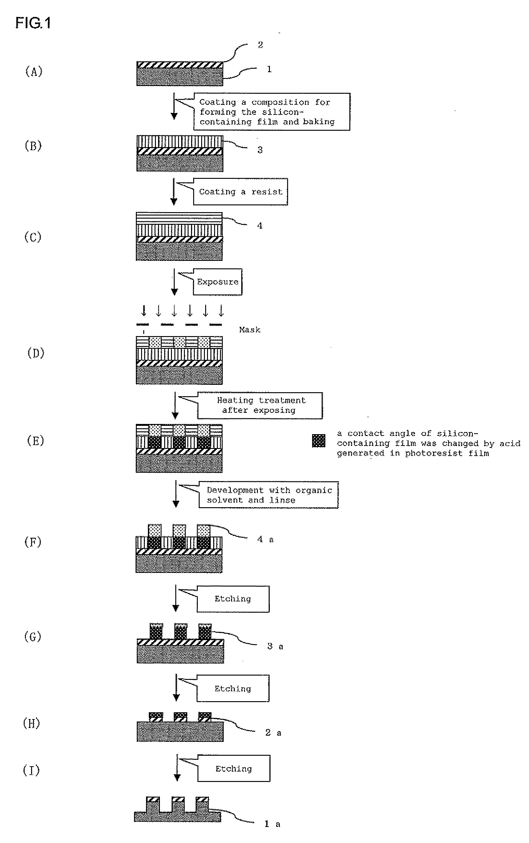
Patterning process

a patterning and process technology, applied in the field of patterning process, can solve the problems of changing the optical system, increasing the cost of the scanner, and poor sustainability of the soft, and achieves the effects of reducing the degree of surface roughness, excellent adhesion, and high precision

Active Publication Date: 2012-11-01
SHIN ETSU CHEM IND CO LTD
View PDF7 Cites 30 Cited by
  • Summary
  • Abstract
  • Description
  • Claims
  • Application Information

AI Technical Summary

Benefits of technology

[0046]As explained above, according to the patterning process of the present invention, a formed negative photoresist pattern has an excellent adhesion; and thus, a pattern without a pattern collapse and with a lower degree of surface roughness can be formed. In addition, the formed photoresist pattern can be transferred by a dry etching process to a silicon-containing resist underlayer film, and then to an organic underlayer film or to a CVD carbon film in order. Especially in the pattern obtained by the ne

Problems solved by technology

However, there are many problems in an F2 lithography; an increase in cost of a scanner due to the use of a large quantity of expensive CaF2 single crystals for a projector lens, extremely p

Method used


Image

  • Patterning process
  • Patterning process
  • Patterning process

Examples


synthesis example 1

[0226]Into a mixture of 120 g of methanol, 1 g of methanesulfonic acid, and 60 g of deionized water was added a mixture of 42.7 g of 2-(4-methoxy carbonyl phenyl)ethyl trimethoxy silane (monomer 10), 13.6 g of methyl trimethoxy silane (monomer 2), and 52.0 g of tetraethoxy silane (monomer 4); and then the resulting mixture was kept at 40° C. for 12 hours for hydrolysis-condensation.

[0227]After the reaction, 100 g of propylene glycol methyl ether was added thereinto and then by-produced alcohol was removed by distillation under reduced pressure. Then, 1000 mL of ethyl acetate and 300 g of propylene glycol methyl ether were added thereinto, and then a water layer was separated. Into the organic layer remained was added 100 mL of ion-exchanged water; the resulting solution was agitated, settled, and separated into layers. This operation was repeated for 3 times. The organic layer remained was concentrated under reduced pressure to obtain 300 g of a propylene glycol methyl ether solutio...

synthesis example 2 to synthesis example 72

[0229]Each synthesis was conducted in the same manner as Synthesis Example 1 by using monomers shown in Table 1-1 to Table 1-4, to obtain the intended compounds (silicon-containing compounds 2 to 72).

TABLE 1-1Silicon -SynthesiscontaingExampleReactive Starting MaterialMwcompound1monomermonomermonomer3,4001104242.7 g52.0 g 13.6 g2monomermonomermonomermonomer3,60021035242.7 g22.8 g 22.8 g13.6 g3monomermonomermonomermonomer2,40031036242.7 g22.8 g 22.8 g13.6 g4monomermonomermonomermonomermonomer3,700411137241.2 g9.9 g22.8 g22.8 g6.8 g5monomermonomermonomermonomermonomer3,900511138241.2 g9.9 g22.8 g22.8 g6.8 g6monomermonomermonomermonomermonomer2,300611139241.2 g9.9 g22.8 g22.8 g6.8 g7monomermonomermonomermonomer2,10071214245.7 g9.9 g52.0 g 6.8 g8monomermonomermonomermonomer3,20081314245.7 g9.9 g52.0 g 6.8 g9monomermonomermonomermonomermonomer3,700913135245.7 g9.9 g22.8 g22.8 g6.8 g10monomermonomermonomermonomermonomer3,3001013134245.7 g9.9 g22.8 g22.8 g6.8 g11monomermonomermonomermonomer...


PUM

PropertyMeasurementUnit
Fractionaaaaaaaaaa
Angleaaaaaaaaaa
Angleaaaaaaaaaa

Abstract

The invention provides a patterning process, comprising at least a step of forming a silicon-containing film on a body to be processed by using a composition for the silicon-containing film, a step of forming, on the silicon-containing film, a photoresist film by using a resist composition, a step of exposing to the photoresist film after heat treatment thereof, and a step of forming a negative pattern by dissolving an unexposed area of the photoresist film by using a developer of an organic solvent; wherein a composition giving the silicon-containing film whose pure-water contact angle in the part corresponding to the exposed area of the photoresist film becomes in the range of 35° or more to lower than 70° after exposure is used as the composition. There can be optimum patterning process as a patterning process of a negative resist pattern to be formed by adopting organic solvent-based development.

Description

BACKGROUND OF THE INVENTION[0001]1. Field of the Invention[0002]The present invention relates to a patterning process including a patterning process to form a negative resist pattern by using an organic solvent developer.[0003]2. Description of the Related Art[0004]In recent years, as LSI progresses toward higher integration and further acceleration in speed, miniaturization of a pattern rule is required. In the light-exposure used as a general technology nowadays, resolution inherent to wavelength of a light source is approaching to its limit. In 1980s, a g-line (436 nm) or an i-line (365 nm) of a mercury lamp was used as an exposure light to be used in a resist pattern forming. As a mean for further miniaturization, a method of shifting to a shorter wavelength of an exposing light was assumed to be effective. As a result, in a mass production process after DRAM (Dynamic Random Access Memory) with 64-megabits (0.25 μm or less of a processing dimension) in 1990s, a KrF excimer laser...

Claims


Application Information

Patent Timeline
IPC IPC(8): G03F7/20C03C25/68
CPCG03F7/0392G03F7/11G03F7/0397G03F7/2041G03F7/0752G03F7/325C07F7/1804G03F7/0042H01L21/0273
Inventor OGIHARA, TSUTOMUUEDA, TAKAFUMIYANO, TOSHIHARU
Owner SHIN ETSU CHEM IND CO LTD
Why Eureka
Try Eureka