
Transparent conductive zinc oxide film, process for production thereof, and use thereof

a technology of transparent conductive zinc oxide and zinc oxide, which is applied in the direction of conductive layers on insulating supports, instruments, conductors, etc., can solve the problems of increasing electrical resistance, deteriorating electrical characteristics, and difficult to achieve the effect of reducing the number of conductive layers, prolonging the material selectivity, and maintaining the durability of the transparent conductive film high

Inactive Publication Date: 2013-02-28
TOSOH CORP
View PDF2 Cites 10 Cited by
  • Summary
  • Abstract
  • Description
  • Claims
  • Application Information

AI Technical Summary

Benefits of technology

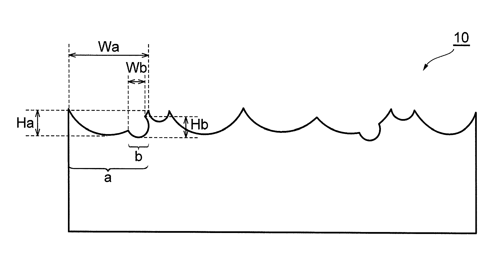
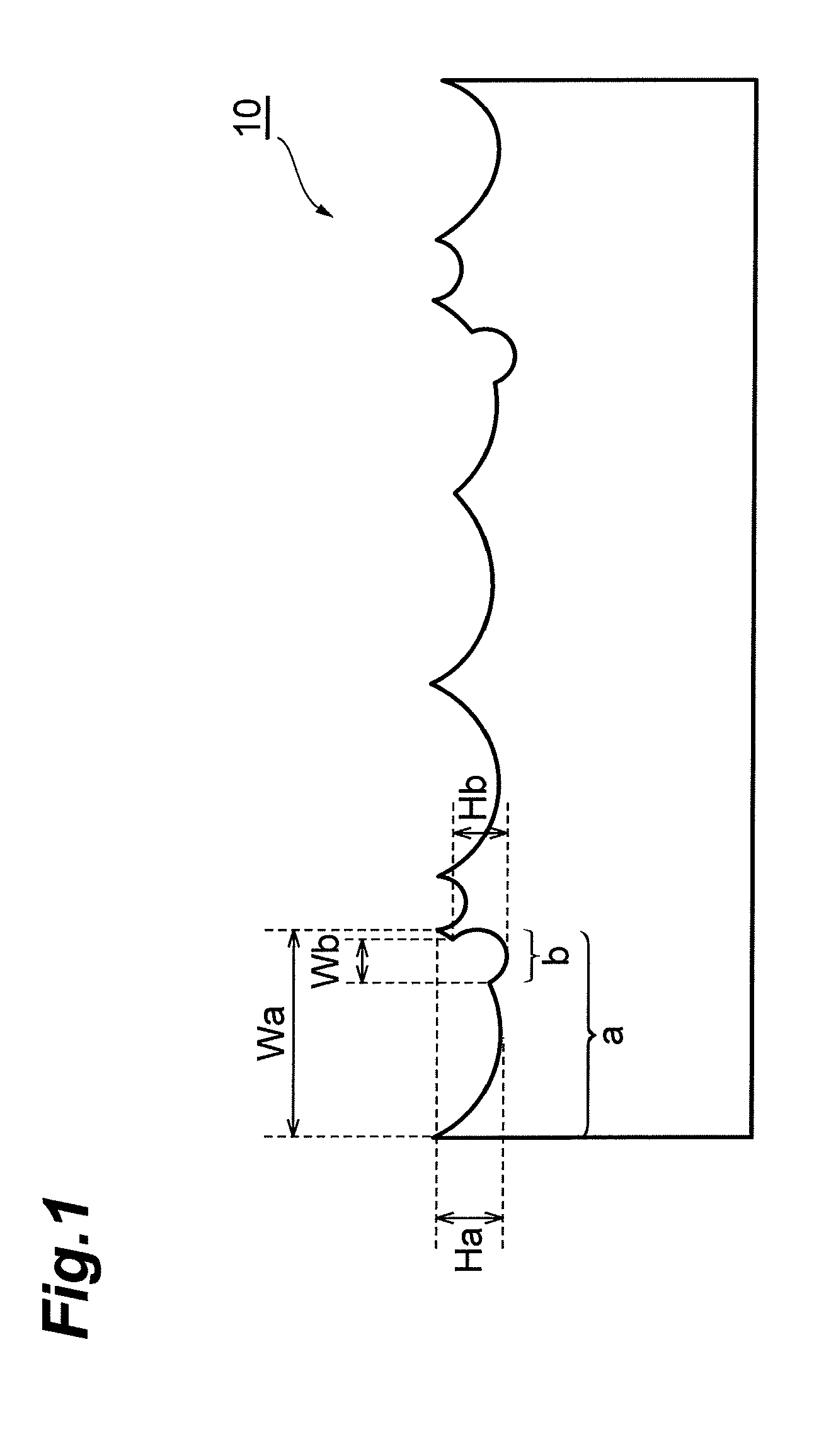
The present invention is about obtaining a transparent conductive film with a specific surface shape that can scatter light in a wide range of wavelengths, such as visible light and near-infrared. This film can be used in optical devices, electron devices, and flexible base plates. Additionally, the film can be formed at low temperatures with high durability. This invention improves the material selectivity and extends the options for applications using transparent conductive films.

Problems solved by technology

In the case of imparting light scattering ability to a transparent conductive film, the approach (2) of the above two methods results in deterioration in electrical characteristics, in particular, increase in electrical resistance, and thus this approach is a very complicated method, when taking into consideration a process for preparing a transparent conductive film.
However, in this Literature, since the textures are formed by molding on a polymer surface using a mold, it is difficult to perform microfabrication below several μm, and a base material on which the textures can be formed has been limited to polymers.
Furthermore, even in the case of forming the concave lens-like textures of a single size on a transparent conductive film, it is necessary to regulate the temperature of a base plate to 300° C. or higher in order to ensure the transparency of the transparent conductive film, and thus the base plate on which the transparent conductive film is formed is limited to materials (glass, metal plate, ceramics and the like) that can withstand high temperatures.

Method used


Image

  • Transparent conductive zinc oxide film, process for production thereof, and use thereof
  • Transparent conductive zinc oxide film, process for production thereof, and use thereof
  • Transparent conductive zinc oxide film, process for production thereof, and use thereof

Examples


examples

[0069]Hereinafter, the present invention will be described in more detail with reference to Examples, but the present invention is not limited to these Examples.

[0070]The number of textures, transmittance and haze rate were recorded as average values by performing each Example five times. The value of the width / depth of the concave lenses shows an average value of values with respect to respective concave lenses observed by AFM, wherein the average value was that determined by selecting an arbitrary 25-μm2 section and determining the average of the values of the whole concave lenses present therein. Herein, it was confirmed by an X-ray diffraction measurement that the crystal structure of the formed transparent conductive film is oriented to (002) plane in the hexagonal system. The measurement conditions are as follows: X-ray source: CuKα, output of X-ray source: 40 kV, 40 mA, and scanning rate: 1° / min.

examples 1 to 8

[0071]As a sputtering target, one prepared by mixing and molding respective powders of ZnO, TiO2 and Al2O3 so that the atomic ratio satisfied those shown in Table 1, then sintering them at 1200° C., and joining the obtained sintered body to a backing plate was used. DC magnetron sputtering was performed under the sputtering conditions of a glass base plate temperature of 200° C., an oxygen partial pressure of 0.1% or less, an argon atmosphere, a sputtering pressure of 0.4 Pa and an input power of 300 W, to thereby produce a film (transparent conductive zinc oxide based film) with a film thickness of 1 nm.

[0072]This film was immersed in hydrochloric acid (liquid temperature: 40° C.) with a hydrogen ion concentration of 0.17 mol / l for seconds and then dried once. Furthermore, the etching was performed two times for 5 seconds, that is, etching was performed for seconds in total, to thereby carry out the surface treatment (Table 2). After such etching, the surface shape was observed by ...

example 9

[0074]A target was prepared by blending respective powders of ZnO, TiO2 and Al2O3 so that the atomic ratio satisfied those shown in Table 1, and subjected to the same film formation, surface treatment and evaluation as in Example 1. Herein, the solution for use in etching was a mixed solution of phosphoric acid / acetic acid (1:1=mol / mol) in which the hydrogen ion concentration was 0.05 mol / l. The results are shown in Tables 3 and 4.


PUM

PropertyMeasurementUnit
Temperatureaaaaaaaaaa
Lengthaaaaaaaaaa
Areaaaaaaaaaaa

Abstract

A transparent conductive zinc oxide based film according to the present invention contains Ti, Al and Zn in such a proportion that satisfies the following formulae (1), (2) and (3) in terms of atomic ratio, and has a plurality of surface textures different in size on a surface, wherein a center-line average surface roughness Ra of the surface of the transparent conductive film is 30 nm to 200 nm, and an average value of widths of the surface textures is 100 nm to 10 μm.0.001≦Ti / (Zn+Al+Ti)≦0.079.  (1)0.001≦Al / (Zn+Al+Ti)≦0.079  (2)0.010≦(Ti+Al) / (Zn+Al+Ti)≦0.080  (3)

Description

TECHNICAL FIELD[0001]The present invention relates to a transparent conductive zinc oxide based film, a method for production thereof and use thereof, and specifically a transparent conductive film having a surface shape useful as an optical device or an electron device and a method for production thereof.BACKGROUND ART[0002]In optical devices and electron devices such as a solar cell, a photodiode, a flat panel display (FPD) and a light-emitting diode (LED), in order to maximally extract their characteristics, a technique for diffusing light is an essential technique, and in particular, a technique for improving light scattering ability at all wavelength regions is essential. As such an approach for scattering light, there are mainly two approaches, which are, for example, as described in Patent Literature 1:[0003](1) an approach for forming fine asperities (hereinafter, textures) on a surface to increase surface roughness, thereby causing optical scattering; and[0004](2) an approa...

Claims


Application Information

Patent Timeline
IPC IPC(8): B32B3/30B05D3/10H01L31/0224C23C14/34
CPCC23C14/08C23C14/086C23C14/34C23C14/5873Y02E10/50Y10T428/24355C23C14/00H01B1/02H01B5/00H01B5/14H01B13/00H01B13/0026H01L31/02366H01L31/0392
Inventor AKIIKE, RYOKURAMOCHI, HIDETOIIGUSA, HITOSHI
Owner TOSOH CORP
Learn More