Laminate, method for producing same, and method for producing device structure using same

Active Publication Date: 2014-02-13
TOYO TOYOBO CO LTD
View PDF2 Cites 82 Cited by
  • Summary
  • Abstract
  • Description
  • Claims
  • Application Information

AI Technical Summary

Benefits of technology

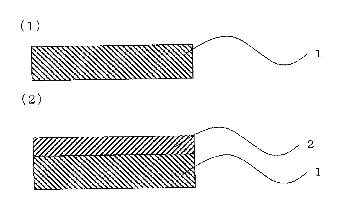
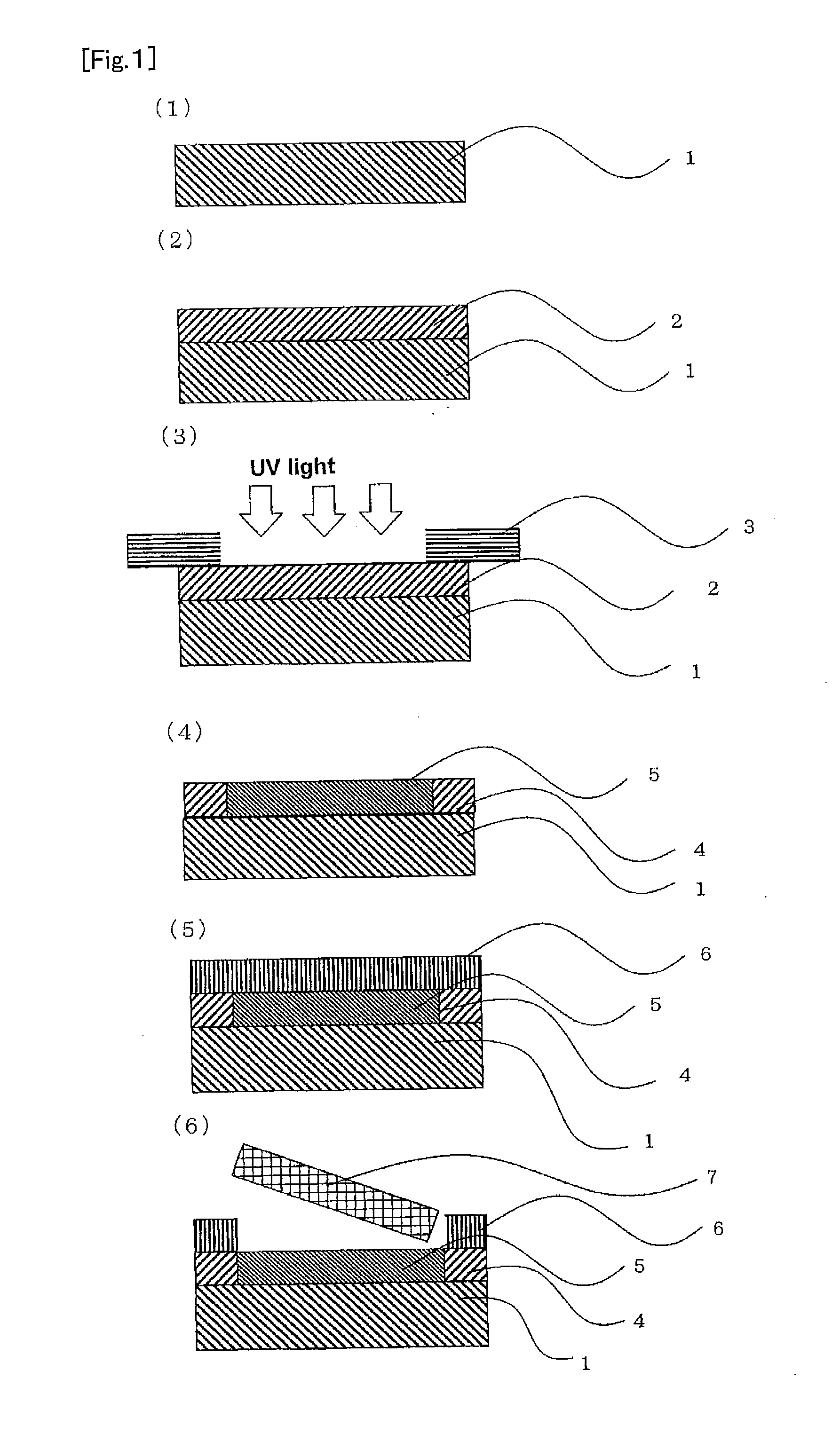
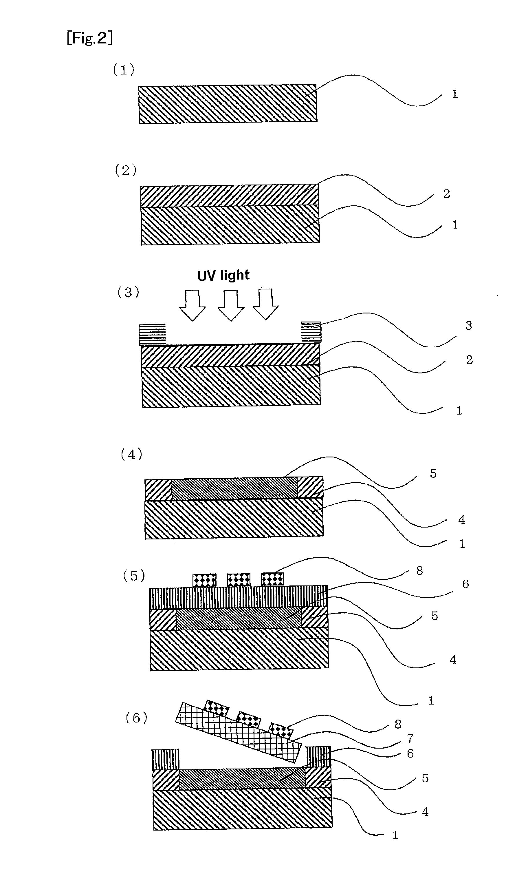
[0032]The laminate obtained by the production method of the present invention is a laminate obtained by sticking one surface of a substrate (a glass plate, a ceramic plate, a silicon wafer, a metal, etc.) and one surface of a polyimide film without an adhesive layer interposed therebetween, and the substrate, and good adhesion parts and easily peeling parts different in adhesion delamination strength of the polyimide film are separated in a previously determined pattern, and therefore it is made possible to easily obtain a device-bearing polyimide film by forming a notch in the polyimide film at the easily peeling part and peeling the polyimide film after a device is fabricated on the polyimide film.
[0033]According to the present invention, a circuit or the like can be formed on a thin polyimide film having insulation properties, flexibility, as well as heat resistance. Further, at the time of fabricating an electronic device by mounting electronic parts, even in the case of a thin polyimide film, the polyimide film is laminated and fixed on a substrate excellent in dimensional stability, and therefore highly precise positioning can be performed and multilayered thin film fabrication and circuit formation can be carried out. Further, the laminate of the present invention is not peeled even if heat is applied during the process, and at the time of peeling from the substrate based on the necessity after device fabrication, the peeling of the polyimide film from the substrate can be smoothly performed. Since the laminate of the present invention is a laminate having delamination strength enough to cause no peeling in the process transfer steps, conventional electronic device fabrication processes can be employed as they are. Particularly, at the time of fabricating a device on the polyimide film, adhesion is excellent and smoothness is also excellent owing to the surface properties of the polyimide film, and therefore device fabrication can be performed stably and precisely. Accordingly, the laminate of the present invention is extremely significant for fabricating an electronic device or the like where a circuit or the like is formed on a thin polyimide film having insulation properties, flexibility, as well as heat resistance.
[0034]According to the present invention, plasma treatment and acid treatment may also be applied to an original polyimide film. The steps for these treatments can be carried out by roll-to-roll process and the treatments can be carried out efficiently. Particularly, a polyimide film roll subjected up to the plasma treatment contains a lubricant, and therefore has a handling property in the form of a roll which is the same as that before plasma treatment. Regarding roll transportation after the acid treatment, the roll transportation is made easy by attaching a protection film coated with a pressure-sensitive adhesive to the surface opposite to the surface which is subjected to the acid treatment. The surface opposite to the surface which is subjected to the acid treatment becomes a surface on which device fabrication is carried out, and therefor

Problems solved by technology

For example, as a material for a base of electronic parts such as information and communication equipments (broadcast equipment, mobile radio equipment, portable communication equipment, etc.), radars, and high speed information processing equipments, ceramics having heat resistance and being capable of dealing with high frequency in a signal band (reaching GHz band) for information and communication equipments have conventionally been used; however, ceramics are not flexible, hard to be made thin, and therefore there is a disadvantage that the fields for which ceramics are applicable are limited.
However, since conventional adhesives and pressure-sensitive adhesives for bonding do not have sufficient heat resistance, they are not currently applicable in the case where the functional device formation temperature is high.
Further, among semiconductor thin films, in the case of forming a Si thin film with a very low coefficient of thermal expansion as low as about 3 ppm/° C. on a polymer film, if the difference between the coefficient of thermal expansion of the film and that of the thin film is high, the stress is accumulated in the thin film and it results in problems of causing deterioration in performance, warping and peeling.
As the polymer film to be stuck to the substrate made of an inorganic substance, films with a low melting point is not suitable in terms of heat resistance, and polymer films made of polyethylene naphthalate, polyethylene terephthalate, polyimide, and polytetrafluoroethylene, glass fiber-reinforced epoxy, and the like are used.
However, a polyimide film generally has a high coefficient of thermal expansion, shows considerable dimensional change owin

Method used


Image

  • Laminate, method for producing same, and method for producing device structure using same
  • Laminate, method for producing same, and method for producing device structure using same
  • Laminate, method for producing same, and method for producing device structure using same

Examples


examples

[0162]Hereinafter, the present invention will be described concretely by way of Examples and Comparative Examples; however, the present invention is not limited to Examples below. The evaluation methods for physical properties in Examples below are as follows.

[0163]The thicknesses of a polyimide film and respective layers (a-layer, b-layer) constituting the polyimide film were measured by using a micrometer (“Millitron 1245D”, manufactured by Feinpruf).

[0164]Strip-like specimens with a size of 100 mm×10 mm in the machine direction (MD direction) and in the transverse direction (TD direction) were cut out from each polyimide film to be measured, and ensile elasticity, tensile strength, and tensile elongation at break of each specimen were measured in the MD direction and in the TD direction, respectively, under conditions of a tension speed of 50 mm / minute and an inter-chuck distance of 40 mm by using a tension testing machine (“Autograph (R); model AG-5000 A”, manufactured by SHIMAD...

production examples 1 and 2

(Preparation of Polyamide Acid Solutions A1 and A2)

[0217]After a reaction container equipped with a nitrogen introduction pipe, a thermometer, and a stirring rod was replaced with nitrogen, 223 parts by mass of 5-amino-2-(p-aminophenyl)benzoxazole and 4416 parts by mass of N,N-dimethylacetamide were added and completely dissolved; and next, 217 parts by mass of pyromellitic acid dianhydride was added thereto in combination with a dispersion obtained by dispersing colloidal silica in dimethylacetamide (“Snowtex (registered trademark) DMAC-ST 30”, manufactured by Nissan Chemical Industries, Ltd.) as a lubricant in an amount such that the addition amount of silica (lubricant) was as shown in Table 1 (mass % to the total weight of the polymer solid matter in the polyamide acid solution), and the mixture was stirred at a reaction temperature of 25° C. for 24 hours to obtain brown and viscous polyamide acid solutions A1 and A2.

TABLE 1ProductionProductionUnitExample 1Example 2Polyamide aci...

production examples 3 and 4

(Preparation of Polyamide Acid Solutions B1 and B2)

[0218]After a reaction container equipped with a nitrogen introduction pipe, a thermometer, and a stirring rod was replaced with nitrogen, 545 parts by mass of pyromellitic anhydride and 500 parts by mass of 4,4′-diaminodiphenyl ether were dissolved in 8000 parts by mass of N,N-dimethylacetamide and the resultant was added thereto, and a dispersion obtained by dispersing colloidal silica in dimethylacetamide (“Snowtex (registered trademark) DMAC-ST 30”, manufactured by Nissan Chemical Industries, Ltd.) was added as a lubricant in an amount such that the addition amount of silica (lubricant) was as shown in Table 2 (mass % to the total weight of the polymer solid matter in the polyamide acid solution), and the mixture was stirred while keeping the temperature at 20° C. or lower for 24 hours to obtain polyamide acid solutions B1 and B2.

TABLE 2ProductionProductionUnitExample 3Example 4Polyamide acidB1B2solutionLubricant typeSilica—Lubr...


PUM

PropertyMeasurementUnit
Temperatureaaaaaaaaaa
Pressureaaaaaaaaaa
Adhesion strengthaaaaaaaaaa

Abstract

The invention provides a laminate of a substrate, a polyimide film, and a coupling treatment layer interposed therebetween, which provides different delamination strengths between the substrate and the polyimide film to form a prescribed pattern. The invention also provides a method for producing such a laminate formed from at least a substrate and a polyimide film, whereby, using a film obtained by plasma treatment of at least the surface facing the substrate as the polyimide film, coupling agent treatment is performed on at least one of the surfaces facing the substrate and the polyimide film to form a coupling treatment layer, deactivation treatment is performed on a portion of the coupling treatment layer to form a pre-determined pattern, and then pressing and heating are performed with the substrate and polyimide film overlapping.

Description

TECHNICAL FIELD[0001]The present invention relates to a method for producing a laminate constituted of a polyimide film and a substrate made of an organic substance (hereinafter, may be referred to simply as “substrate”). Specifically, the present invention relates to a method for producing a laminate by temporarily or semipermanently sticking a polyimide film to an inorganic basal plate as a substrate, and the laminate is useful at the time of forming a device such as a semiconductor device, a MEMS device, or a display device, which is made of a thin film and requires fine processing, on a polyimide film surface. More specifically, the laminate according to the present invention is a laminate constituted of a thin polyimide film excellent in heat resistance and insulation properties and a substrate made of an inorganic substance (e.g., one kind selected from a glass plate, a ceramic plate, a silicon wafer, and a metal plate) having a coefficient of thermal expansion which is substa...

Claims


Application Information

Patent Timeline
IPC IPC(8): B32B38/10B32B7/06B32B38/00
CPCB32B38/10B32B7/06B32B38/0004B29C59/14B29C65/02B29C65/1406B29C65/1432B29C65/1496B29C65/76B29C66/028B29C66/1122B29C66/41B29C66/43B29C66/71B29C66/73111B29C66/73117B29C66/7315B29C66/73161B29C66/7352B29C66/7392B29C66/7394B29C66/7465B29C66/9121B29C66/91216B29C66/91311B29C66/91313B29C66/91315B29C66/9141B29C66/91445B29C66/919B29C66/953B29C2035/0827B29K2995/0072B32B27/08B32B27/16B32B27/281B32B27/34B32B38/0008B32B2255/10B32B2255/26B32B2307/306B32B2307/71B32B2307/734B32B2307/748B32B2315/08B32B2379/08B32B2457/00C08G73/105C08G73/1067C08G73/1071C08G73/1085C08G73/22C08L79/08Y10T156/10Y10T428/24802Y10T428/24851Y10T428/31725B29K2079/08B32B37/00
Inventor OKUYAMA, TETSUOOUYA, KAZUYUKITSUCHIYA, TOSHIYUKIWATANABE, NAOKIMAEDA, SATOSHI
Owner TOYO TOYOBO CO LTD
Why Eureka
Try Eureka