Semiconductor device
a technology of semiconductors and semiconductors, applied in logic circuits, pulse automatic control, pulse techniques, etc., can solve the problems of driver circuit including transistor malfunction, increase manufacturing costs, etc., and achieve the effects of preventing malfunction, low power consumption, and superior stability of electrical characteristics
- Summary
- Abstract
- Description
- Claims
- Application Information
AI Technical Summary
Benefits of technology
Problems solved by technology
Method used
Image

Examples
embodiment 1
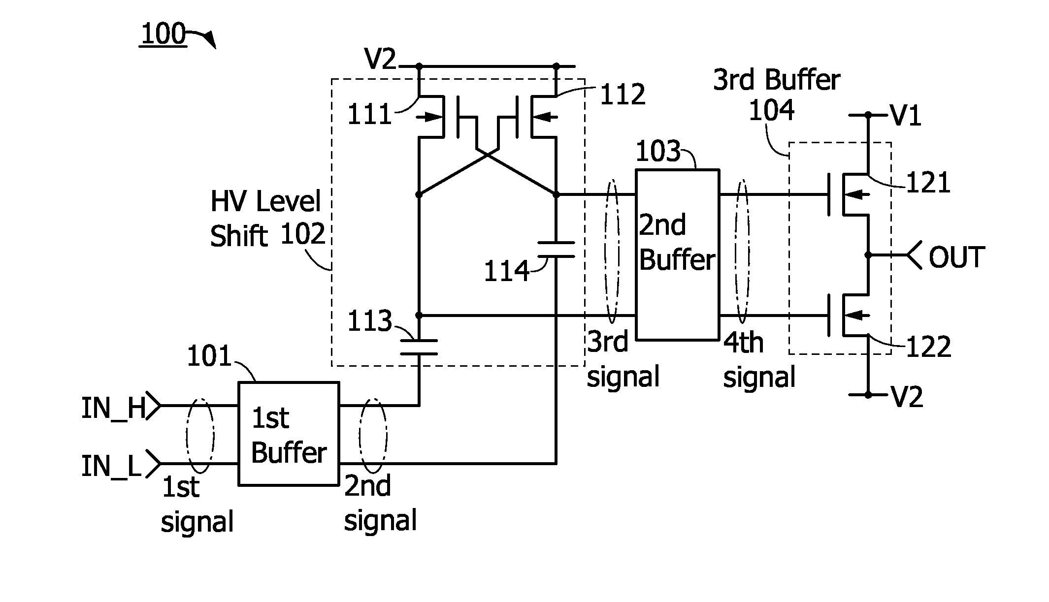
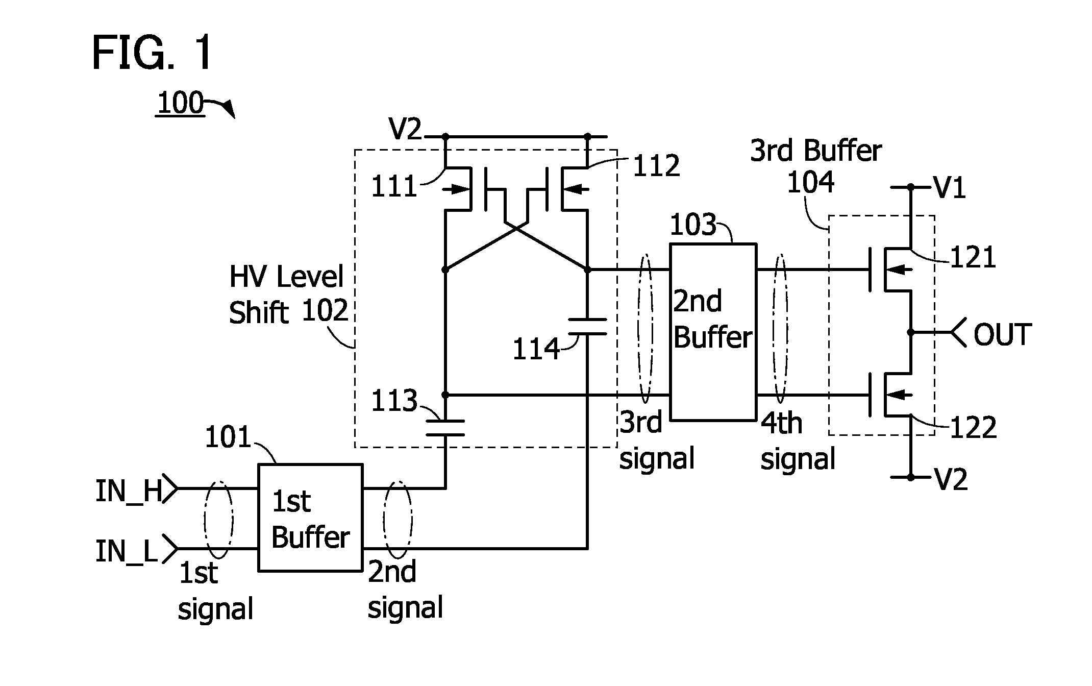
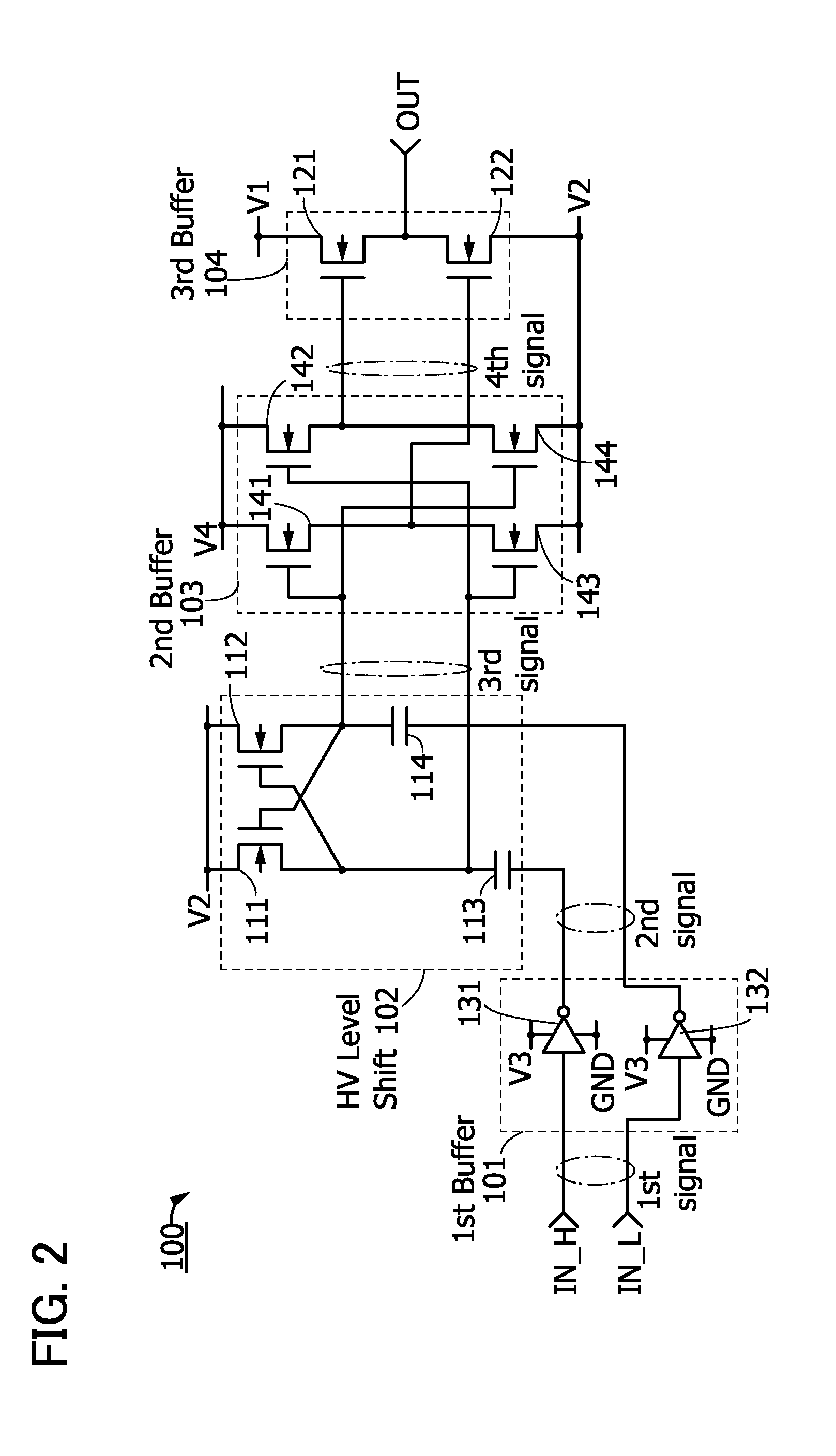
[0046]In this embodiment, a circuit configuration and operation of a semiconductor device according to one embodiment of the invention to be disclosed will be described with reference to FIG. 1.
[0047]Note that a semiconductor device means a circuit having a semiconductor element (e.g., a transistor or a diode) and a device having the circuit. The semiconductor device also means any device that can function by utilizing semiconductor characteristics. For example, an integrated circuit, a chip having an integrated circuit, a display device, a light-emitting device, a lighting device, and an electronic device are all semiconductor devices.
[0048]FIG. 1 is a block diagram of a semiconductor device. A semiconductor device 100 shown in FIG. 1 includes a buffer circuit 101 (also referred to as a first buffer circuit and expressed as 1st Buffer in the drawing), a level-shift circuit 102 (expressed as HV Level Shift in the drawing), a buffer circuit 103 (also referred to as a second buffer ci...
embodiment 2
[0108]In this embodiment, an oxide semiconductor that can be used for the semiconductor layer of the transistor having the same conductivity type described in the above embodiment will be described.
[0109]An oxide semiconductor used for a channel formation region in the semiconductor layer of the transistor preferably contains at least indium (In) or zinc (Zn). In particular, the oxide semiconductor preferably contains both In and Zn. A stabilizer for strongly bonding oxygen is preferably contained in addition to In and Zn. As the stabilizer, at least one of gallium (Ga), tin (Sn), zirconium (Zr), hafnium (Hf), and aluminum (Al) may be contained.
[0110]As another stabilizer, one or plural kinds of lanthanoid such as lanthanum (La), cerium (Ce), praseodymium (Pr), neodymium (Nd), samarium (Sm), europium (Eu), gadolinium (Gd), terbium (Tb), dysprosium (Dy), holmium (Ho), erbium (Er), thulium (Tm), ytterbium (Yb), and lutetium (Lu) may be contained.
[0111]As the oxide semiconductor used f...
embodiment 4
[0157]In this embodiment, application examples of the semiconductor device described in the foregoing embodiment to an electronic component and to an electronic device including the electronic component will be described with reference to FIGS. 10A and 10B and FIGS. 11A and 11B.
[0158]FIG. 10A illustrates an example where the semiconductor device described in the foregoing embodiment is used to make an electronic component. Note that an electronic component is also referred to as a semiconductor package or an IC package. For the electronic component, there are a variety of standards and names corresponding to the direction of terminals or the shape of terminals; hence, one example of the electronic component will be described in this embodiment.
[0159]A semiconductor device including the transistors illustrated in FIGS. 7A and 7B, FIGS. 8A and 8B, and FIGS. 9A and 9B of Embodiment 3 undergoes the assembly process (post-process) and is completed by using a combination of components det...
PUM
 Abstract
Description
Claims
Application Information
 - R&D
- Intellectual Property
- Life Sciences
- Materials
- Tech Scout
- Unparalleled Data Quality
- Higher Quality Content
- 60% Fewer Hallucinations
Browse by: Latest US Patents, China's latest patents, Technical Efficacy Thesaurus, Application Domain, Technology Topic, Popular Technical Reports.
© 2025 PatSnap. All rights reserved.Legal|Privacy policy|Modern Slavery Act Transparency Statement|Sitemap|About US| Contact US: help@patsnap.com