

Cleaning liquid for semiconductor elements and cleaning method using same
- Summary
- Abstract
- Description
- Claims
- Application Information
AI Technical Summary
Benefits of technology
Problems solved by technology
Method used
Image

Examples
examples
[0040]Hereinafter, the present invention will be more specifically described by way of examples and comparative examples. However, the present invention is not limited to the examples.
[0041]The state of removal of materials and damage were evaluated by means of SEM observation. As an SEM apparatus, an ultra-high resolution field-emission scanning electron microscope SU9000 manufactured by Hitachi High-Technologies Corporation was used.
[0042]An acid-added cleaning liquid was prepared by mixing a cleaning liquid with 10% by mass of an aqueous solution of hydrofluoric acid at a mass ratio of 100:2. A semiconductor element having a copper wiring was immersed in the hydrofluoric acid-added cleaning liquid at a predetermined temperature for a predetermined period of time, and damage to the copper was observed by means of SEM observation.
[0043]A composition obtained by mixing a cleaning liquid with titanium powder at a mass ratio of 100:0.005 was heated in a constant temperature water tank...
examples 1-22
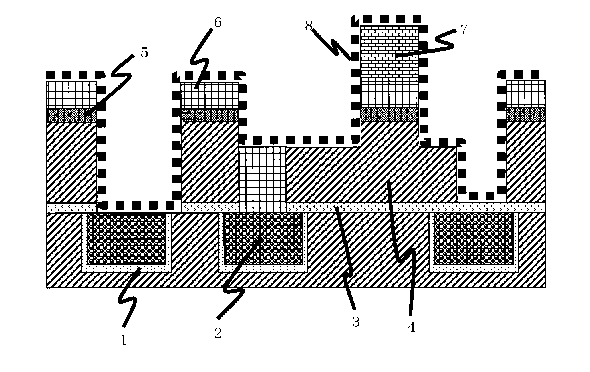
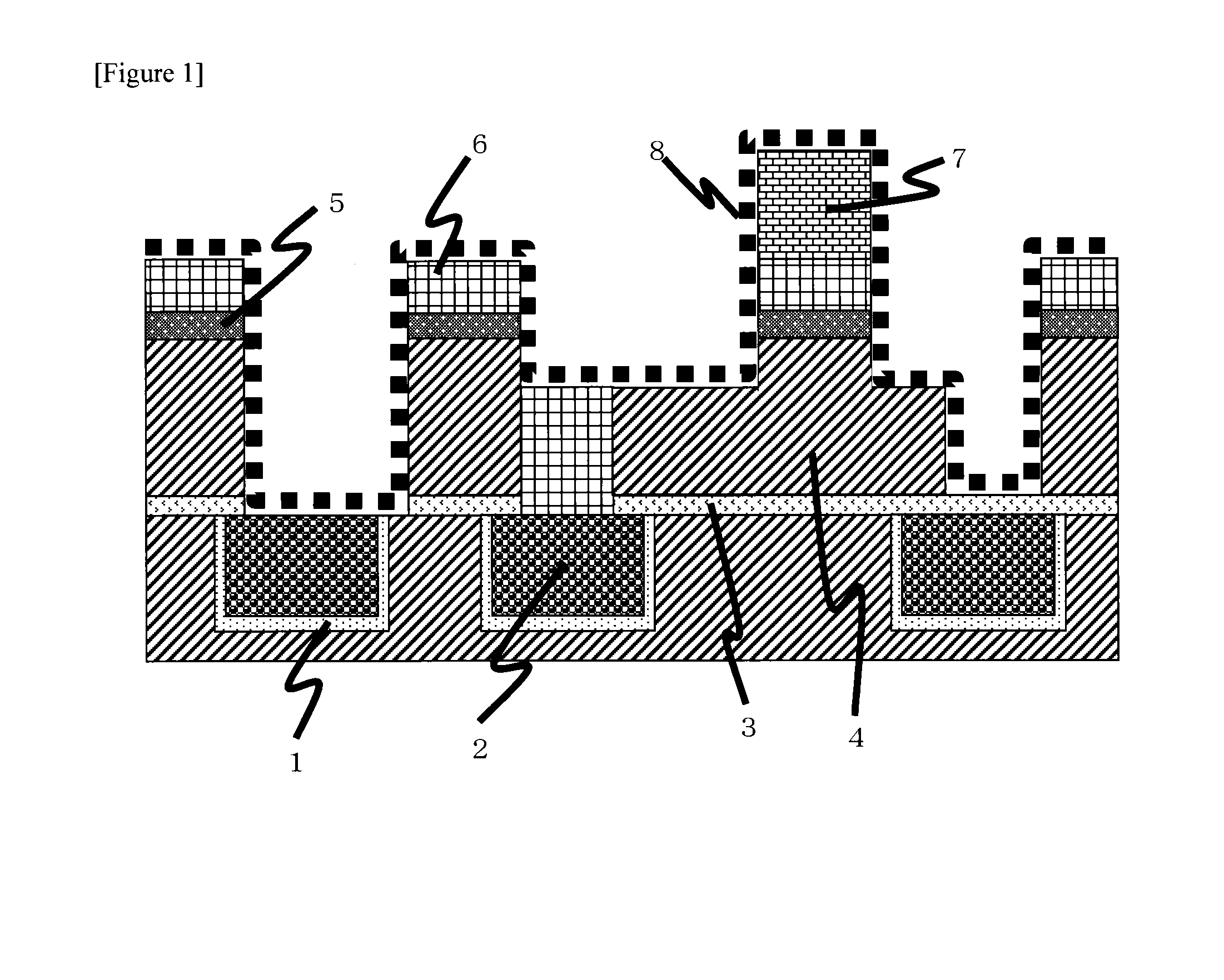
[0078]In the test, a semiconductor element having a cross-sectional surface of a wiring structure as shown in FIG. 1 was used. In order to remove the hard mask 5 that is TiN, the organosiloxane-based thin film 6, the dry etching residue 8 and the photoresist 7, the semiconductor element was immersed in a cleaning liquid described in Table 1 at a temperature and for time described in Table 2, and after that, it was rinsed with ultrapure water and dried by means of dry nitrogen gas jet. The semiconductor element after cleaning was observed by SEM to judge the state of removal of each of the hard mask 5, the organosiloxane-based thin film 6, the dry etching residue 8 and the photoresist 7 and damage to each of the copper 2, tantalum (Ta) / tantalum nitride (TaN) that is the barrier metal 1, silicon carbide that is the barrier dielectric film 3 and carbon-doped silicon oxide that is the low-dielectric-constant interlayer dielectric film 4. In addition, the semiconductor element was immers...
PUM
| Property | Measurement | Unit |
|---|---|---|
| Fraction | aaaaa | aaaaa |
| Percent by mass | aaaaa | aaaaa |
| Percent by mass | aaaaa | aaaaa |
Abstract
Description
Claims
Application Information