Solar cell and production method therefor

Active Publication Date: 2016-11-10
MATERIAL CONCEPT
View PDF3 Cites 1 Cited by
  • Summary
  • Abstract
  • Description
  • Claims
  • Application Information

AI Technical Summary

Benefits of technology

[0088]The present invention represents a silicon solar cell in which a metal oxide layer formed on a silicon substrate which is configured by combining each element of the aforementioned (a) to (c), and copper wiring is formed on that metal oxide layer. The above metal oxide layer can minimize interdiffusion between the silicon substrate and the copper wiring. Further, the aforementioned metal oxide layer has excellent adhesiveness with both the copper wiring and the silicon substrate, and has low electrical resistance. Therefore, good ohmic contact characteristics with less losses when electric current flows between the copper wiring and the silicon substrate can be obtained. Inexpensive copper-based metal wiring used therein can allow for large cost reduction. Low wiring and low contact resistances can reduce theseries resistance of a cell, leading to improved conversion efficiency. Further, th

Problems solved by technology

This will be accompanied by significant power loss when electric power generated inside a silicon cell is retrieved outside.
However, copper will diffuse into silicon through the entire interface layer or through the grain boundary in the interface layer as diffusion routes, and thus good diffusion barrier characteristics can not be obtained for the interface layer.
Therefore, disadvantageously, the long-term reliability, which is a requirement for a solar cell, is inferior.
However, when a collector electrode is sintered at a high temperature, a TCO is reduced by silicon to change its properties, and insulating SiO2 is formed at an interface because an oxide to become a TCO is less stable than SiO2.
Therefore, disadvantageously, the ohmic contact characteristics are deteriorated.
Further, disadvantageously, the adhesiveness between copper wiring and a transparent conducting film will be insufficient.
However, these prior art documents do not include any statement with regard to whether or not a Ti oxide can serve as a diffusion barrier layer between copper and silicon in a silicon solar cell having copper wiring, neither does any statement of implementation of it.
Therefore, a problem is that the electrical conductivity between copper and a Si substrate, i.e., good ohmic contact characteristics can not be obtained when these interface layers are applied to solar cells.
However, a problem is that the silicide non-uniformly enters into an emitter layer near the surface of the Si substrate due to the non-uniform

Method used


Image

  • Solar cell and production method therefor
  • Solar cell and production method therefor

Examples


Example

Example 1

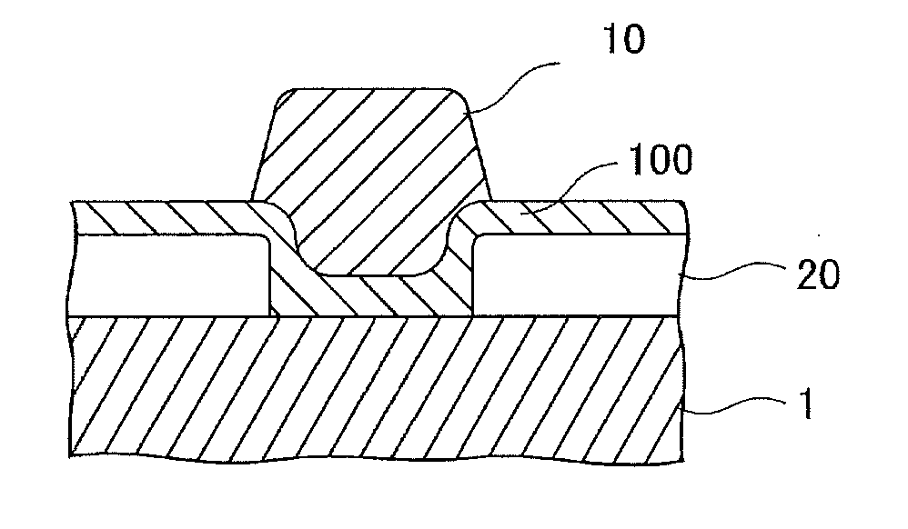
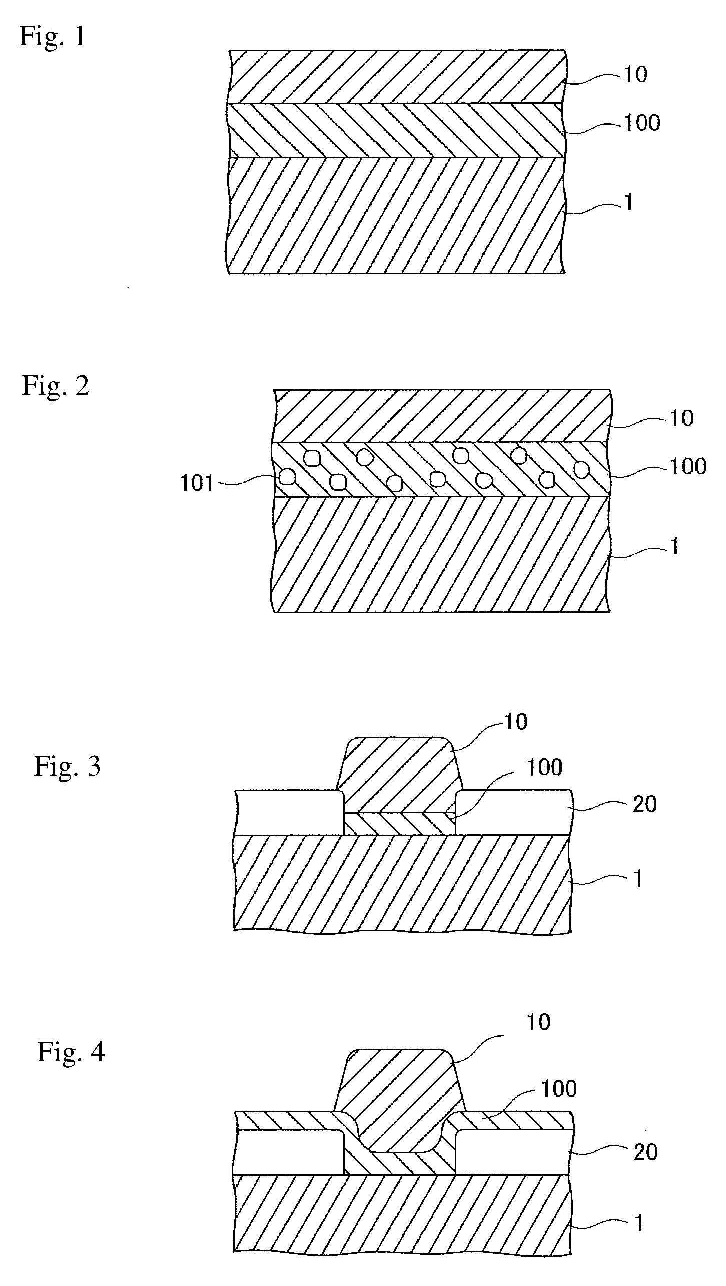
[0137]A monocrystalline p-type silicon wafer with a dimension of 156 mm square and 0.2 mm thickness was used as a silicon substrate. The p-type impurity was boron (B) and the impurity concentration was about 1×1016 cm-3. The upper surface of this wafer was etched with a KOH solution, and a texture structure with unevenness was formed. Subsequently, after POCl3 was applied to the upper surface, heat-treatment was performed at high temperature to diffuse phosphorus (P) into silicon, thereby forming an n+ region. The concentration of P was up to about 1×1019 cm-3. A silicon substrate having n-p junction was produced in this way.

[0138]As a raw material solution, a mixture solution comprising a Ti-based alkoxide compound, an Nb-based alkoxide compound, and a solvent was prepared. A slit coating device was used to uniformly apply the raw material solution on the silicon substrate. The substrate on which the solution had been applied was dried at about 200° C., and then calcined b...

Example

Example 2

[0149]An antireflection SiN film with a thickness of 80 nm was deposited on the surface of the silicon substrate having n-p junction from Example 1 by the plasma-enhanced chemical vapor-phase deposition method (PECVD). Then, a portion in which copper wiring was to be formed was removed by the laser ablation method.

[0150]A metal oxide and copper wiring were formed on the above silicon substrate on which the antireflection film had been formed, under similar conditions as in Example 1.

[0151]The electric resistivity of the copper wiring was 3.3 μΩcm, the adhesion strength of the copper wiring was 1.9 N / mm, and the visible light transmittance of the metal oxide layer at a wavelength of 500 nm was 92%. Further, after a heat treatment at 500° C. for 30 minutes, copper atoms were found to be below the detection limit, and interdiffusion of Cu and Si was not observed, indicating that good diffusion barrier characteristics were obtained.

Example

Example 3

[0152]After forming a metal oxide layer comprising copper, titanium, niobium on a silicon substrate at a thickness of about 30 nm under similar conditions as in Example 1, heat treatment was performed for 10 minutes at a temperature of 500° C. and an ambient pressure of 104 Pa under a reducing atmosphere in which 5% hydrogen was mixed in nitrogen. In the structure after the heat treatment, copper particles were precipitated in the metal oxide comprising titanium and niobium. The mean diameter of the copper particles was about 5 nm.

[0153]Then, copper wiring was formed by the method described in Example 1. The electric resistivity of the copper wiring was 3.0 μΩcm, the adhesion strength of the copper wiring was 4.2 N / mm, and the visible light transmittance of the metal oxide layer at a wavelength of 500 nm was 90%. Further, after a heat treatment at 500° C. for 30 minutes, copper atoms were found to be below the detection limit, and interdiffusion of Cu and Si was not observe...


PUM


Abstract

The present invention is provided with an interface layer that minimizes interdiffusion between a silicon substrate and copper electrode wiring that are used as a solar cell, that improves the adhesive properties of copper wiring, and that is used to obtain ohmic contact characteristics. This silicon solar cell comprises a silicon substrate and is provided with a metal oxide layer that is formed on the silicon substrate and wiring that is formed on the metal oxide layer and that comprises mainly copper. The metal oxide layer contains (a) one of either titanium or manganese, (b) one of vanadium, niobium, tantalum, or silicon, and (c) at least one of copper and nickel. In addition, the metal oxide layer comprises copper or nickel as metal particles that are diffused in the interior of the metal oxide layer.

Description

TECHNICAL FIELD[0001]The present invention relates to a silicon solar cell comprising copper-based metal wiring, and also relates to a method of manufacturing the above silicon solar cell.BACKGROUND ART[0002]In a solar cell having a silicon substrate, silver is commonly used for collector electrode wiring. Considering that the cost of silver as a raw material, which accounts for 20% or more of the total material cost of a solar cell, has been soaring in recent years, substitution of lower cost copper for silver has been demanded in order to reduce the price of a solar cell.[0003]However, copper (Cu) and silicon (Si) undergo interdiffusion to form copper silicide. Further, copper rapidly diffuses into a region of silicon to form an acceptor level at an energy position deep in the band gap of silicon. Since these phenomena may be responsible for deteriorated properties of a solar cell, a diffusion barrier layer is required between copper and silicon in order to minimize interdiffusion...

Claims


Application Information

Patent Timeline
IPC IPC(8): H01L31/0224H01L31/068H01L31/18H01L31/0216
CPCH01L31/022466H01L31/1884H01L31/068H01L31/02168H01L31/022425Y02E10/547
Inventor KOIKE, JUNICHISUTOU, YUJIANDO, DAISUKEHOANG, TRI HAI
Owner MATERIAL CONCEPT
Why Eureka
Try Eureka