Unlock instant, AI-driven research and patent intelligence for your innovation.
High permittivity silicate gate dielectric
Inactive Publication Date: 2005-01-11
TEXAS INSTR INC
View PDF39 Cites 57 Cited by
Summary
Abstract
Description
Claims
Application Information
AI Technical Summary
This helps you quickly interpret patents by identifying the three key elements:
Problems solved by technology
Method used
Benefits of technology
The present invention comprises a semiconductor device structure utilizing a metal silicate gate dielectric layer, and a method for making the same. With the present invention, a metal silicate gate dielectric may be formed with a dielectric constant substantially higher than that of either conventional thermal silicon dioxide or silicon nitride dielectrics, and thus the metal silicate dielectric layer may be made substantially thicker than a conventional gate dielectric with equivalent field effect. However, it is believed that the present invention largely avoids disadvantages, such as interfacial silicon dioxide formation and high interface state densities, that are found with conventional alternative dielectrics.
The present invention generally avoids the problems of other alternative dielectrics by employing an oxidized dielectric material comprising a significant amount of silicon, particularly at the silicon / dielectric interface. In one preferred embodiment, a graded silicate layer is formed, such that near the silicon interface the silicate layer has a large SiO2 component, while the upper portion of the silicate layer has a large metal oxide component. Such a structure employs primarily SiO2 bonding at the silicon interface, with resulting low interface state densities. However, the high atomic number metal included in the silicate layer can significantly increase the dielectric constant of the film. The present invention also provides for amorphous silicate gate dielectrics, which have dense microstructures and avoid many of the problems associated with grain boundaries in polycrystalline dielectrics.
Problems solved by technology
Although transistor design and fabrication is a highly complex undertaking, the general structure and operation of a transistor are fairly simple.
Unfortunately, field effect semiconductor devices produce an output signal that is proportional to the width of the channel, such that scaling reduces their output.
Although further scaling of devices is still possible, scaling of the gate dielectric thickness has almost reached its practical limit with the conventional gate dielectric material, silicon dioxide.
Further scaling of silicon dioxide gate dielectric thickness will involve a host of problems: extremely thin layers allow for large leakage currents due to direct tunneling through the oxide; because such layers are formed literally from a few layers of atoms, exacting process control is required to repeatably produce such layers; uniformity of coverage is also critical because device parameters may change dramatically based on the presence-or absence of even a single monolayer of dielectric material; and finally, such thin layers form poor diffusion barriers to impurities.
Researchers have found formation of such metal oxides as gate dielectrics to be problematic.
The presence of this interfacial oxide layer increases the effective oxide thickness, reducing the effectiveness of the alternative gate dielectric approach.
Method used
Image
Click on the blue label to locate the original text in one second.
Reading with bidirectional positioning of images and text.
Examples
embodiment 1
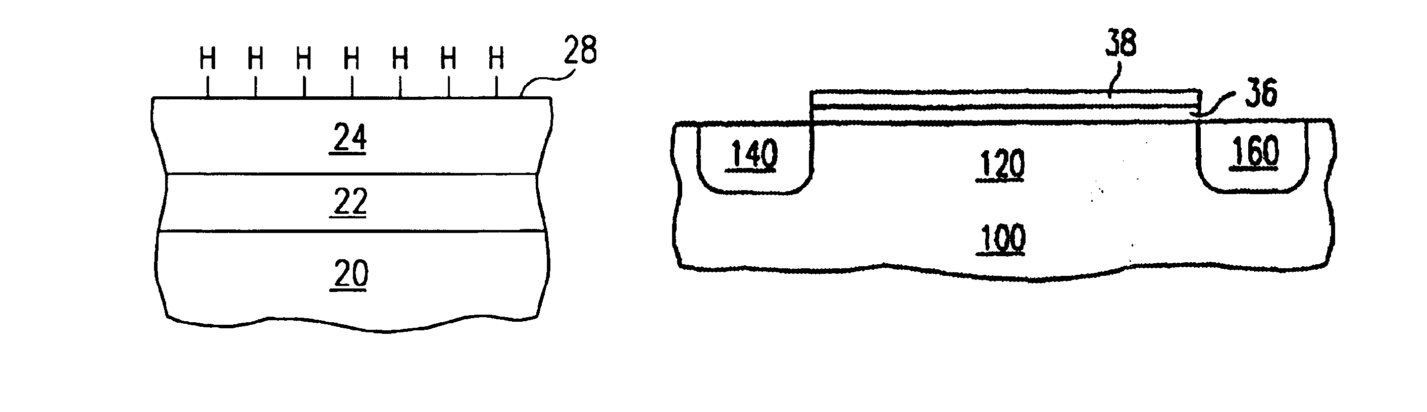
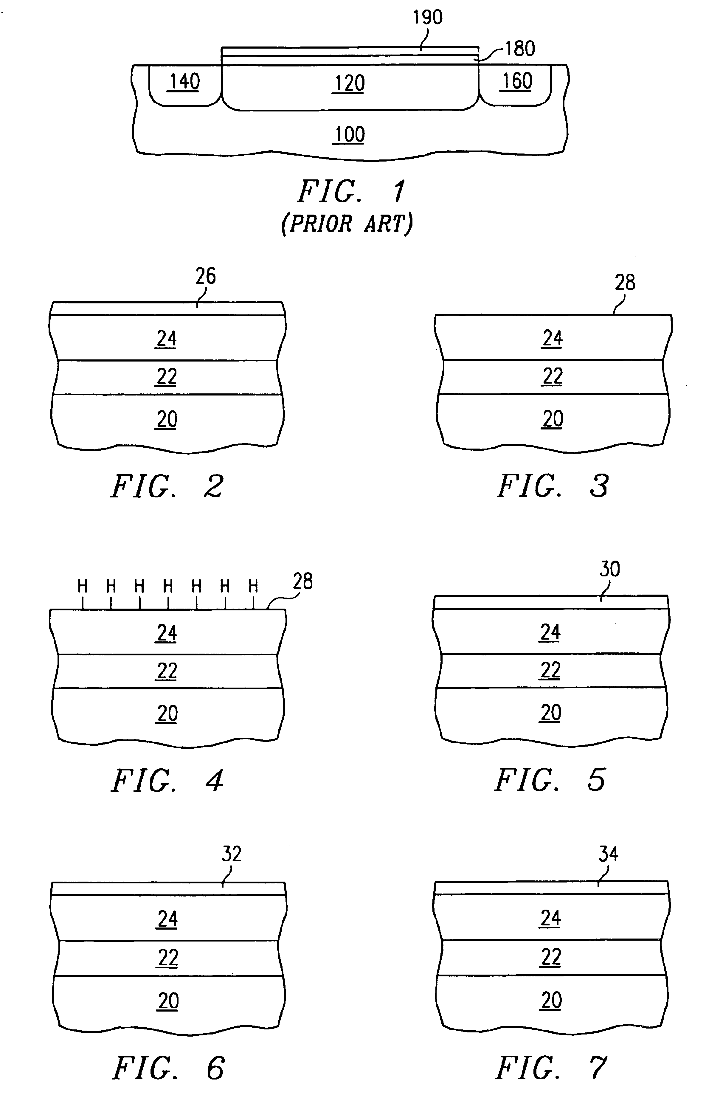
In one embodiment according to the invention, a metal silicate gate dielectric is formed by depositing metal on a clean Si surface, annealing this structure to form a metal silicide, oxidizing the silicide layer, and annealing this structure. In this embodiment, a substrate such as shown in either FIG. 3 or FIG. 4 is used. If surface 28 is passivated as shown in FIG. 4, the substrate can be briefly heated to above 500° C. in vacuum or an inert ambient to remove the passivation.
Referring to FIG. 6, a metal layer 32 (e.g. zirconium or hafnium) is deposited directly on surface 28, e.g. by sputtering, evaporation, chemical vapor deposition (CVD) or plasma CVD. Sputter deposition is preferably done with a low-energy plasmasystem, such as collimated or long-throw sputtering; it should be noted that low deposition rates (e.g. on the order of a few angstroms per second) are preferred, as the total thickness to be deposited is small and uniformity is desired. For an 8″ wafer, deposition may...
embodiment 2
In a second embodiment according to the invention, a metal silicate gate dielectric is formed by depositing metal on a substrate in an oxidizing ambient, followed by annealing. This embodiment preferably utilizes a substrate prepared by one of the methods corresponding to FIG. 2, 3, or 4, and the metal may be deposited by one of the methods described in Embodiment 1, with the following differences.
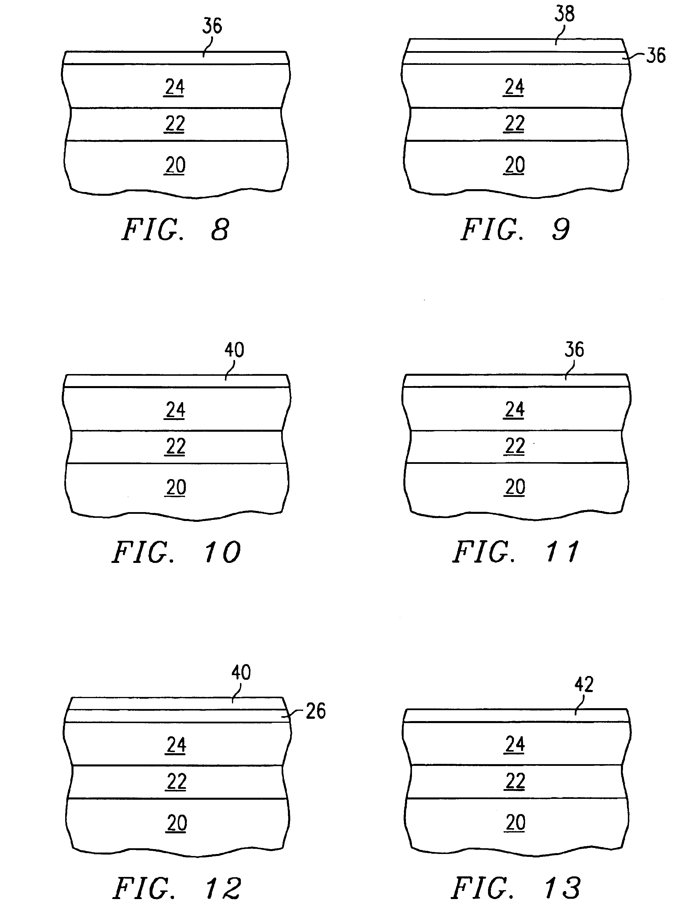
Referring to FIG. 10, an oxidized metal layer 40 may be deposited on a clean Si surface by sputtering as described above. However, some amount of controlled oxygen activity is used to at least partially oxidize layer 40 as metal is supplied to the substrate. For example, O2 or H2O+H2 may be introduced near the substrate during sputtering with Ar, with an O2 flow rate of about one-tenth that of the Ar flow rate. For a metal deposition rate of 0.1 nanometers per second, the oxidizing gas is preferably introduced from 0 to 5 seconds after the start of the deposition process.
If oxidized metal ...
embodiment 3
In a third embodiment according to the invention, a metal silicate gate dielectric is formed by depositing both metal and silicon on the substrate in an oxidizing ambient, followed by annealing. In this embodiment, the substrate preparation may be chosen as any of those shown in FIGS. 2-5. As this method generally does not rely on silicon from the substrate as a component of the silicate film, a surface that limits oxidation of the substrate, such as the diffusion barrier surface of FIG. 5, is preferred. The metal and silicon may be deposited by one of the methods described in Embodiment 1, with the following differences.
Referring to FIG. 13, an oxidized metal and silicon layer 42 may be deposited on a clean Si surface by sputtering as described in Embodiment 2 for the deposition of oxidized metal layer 40. The deposition of both metal and silicon is accomplished by replacing the metal target with an appropriate silicide target. The disadvantage of this method is that deposition of ...
PUM
Abstract
A field effectsemiconductor device comprising a high permittivitysilicategate dielectric and a method of forming the same are disclosed herein. The device comprises a silicon substrate 20 having a semiconducting channel region 24 formed therein. A metalsilicategate dielectric layer 36 is formed over this substrate, followed by a conductive gate 38. Silicate layer 36 may be, e.g., hafniumsilicate, such that the dielectric constant of the gate dielectric is significantly higher than the dielectric constant of silicon dioxide. However, the silicate gate dielectric may also be designed to have the advantages of silicon dioxide, e.g. high breakdown, low interface state density, and high stability. The present invention includes methods for depositing both amorphous and polycrystalline silicate layers, as well as graded composition silicate layers.
Description
FIELD OF THE INVENTIONThis invention relates generally to semiconductor device structures and methods for forming such, and more specifically to such structures and methods related to gate dielectrics for field effect devices formed on integrated circuits.BACKGROUND OF THE INVENTIONSemiconductor devices such as field effect transistors are common in the electronics industry. Such devices may be formed with extremely small dimensions, such that thousands or even millions of these devices may be formed on a single-crystal silicon substrate or “chips” and interconnected to perform useful functions in an integrated circuit such as a microprocessor.Although transistor design and fabrication is a highly complex undertaking, the general structure and operation of a transistor are fairly simple. With reference to FIG. 1, a simplified field effect transistor is shown in cross-section. In a field effect transistor a portion of the substrate 100 near the surface is designated as the channel 12...
Claims
Application Information
Patent Timeline
Application Date:The date an application was filed.
Publication Date:The date a patent or application was officially published.
First Publication Date:The earliest publication date of a patent with the same application number.
Issue Date:Publication date of the patent grant document.
PCT Entry Date:The Entry date of PCT National Phase.
Estimated Expiry Date:The statutory expiry date of a patent right according to the Patent Law, and it is the longest term of protection that the patent right can achieve without the termination of the patent right due to other reasons(Term extension factor has been taken into account ).
Invalid Date:Actual expiry date is based on effective date or publication date of legal transaction data of invalid patent.