Method of manufacturing a semiconductor device with fluorine concentration

a technology of semiconductor devices and concentration, applied in semiconductor devices, electrical equipment, transistors, etc., can solve the problems of reduced yield, increased process time, and low-priced glass used for a substrate, so as to reduce the process time, and reduce the amount of fluorine taken into the film

Inactive Publication Date: 2005-04-05
SEMICON ENERGY LAB CO LTD
View PDF34 Cites 45 Cited by
  • Summary
  • Abstract
  • Description
  • Claims
  • Application Information

AI Technical Summary

Benefits of technology

From the above results, the inventors of the present invention found that, in crystallization of an amorphous silicon film, the contents of oxygen elements and nitrogen elements in the amorphous silicon film are not so large issues and that the content of fluorine elements is what largely influences the crystallization. Generally, cleaning is performed using fluorine compound gas such as ClF3 or NF3 in a film forming chamber for forming a silicon-based film. Therefore, fluorine remains while being adhered to inner walls and the like of the film forming chamber. The inside of the film forming chamber is generally coated before film formation in order to prevent the residual fluorine from being taken into the film. In this experiment, the film formation is performed in the state that the film forming chamber has been coated with a thickness of 3 μm or more, but the amount of fluorine contained in an amorphous silicon film was large in case of the film formation of the amorphous silicon film performed with only SiH4 gas. However, according to the present invention, the amount of fluorine taken into the film can be suppressed by forming an amorphous silicon film using SiH4 gas diluted with hydrogen. Further, a sufficiently crystallized silicon film can be obtained by crystallizing the amorphous silicon film. Consequently, according to the present invention, coating processing time after cleaning can be shortened, and thus, a reduction in process time can be expected.

Problems solved by technology

Furthermore, in recent years, low-priced glass has been used for a substrate in order to manufacture a display device with a large screen at a low price.
Therefore, because a substrate is conveyed, there have been problems such as the increase in process time and the reduction in yield due to conveyance trouble.
Further, even if continuous formation (formation of lamination by continuously forming films without exposure to an atmosphere) from the formation of the base film through the formation of the amorphous silicon film can be performed in a single chamber, since the amorphous silicon film formed in the single chamber contains a large amount of impurities such as oxygen, nitrogen and fluorine which are factors of obstructing crystallization, it has been difficult to obtain a satisfactory crystalline silicon film by using a known crystallization technique.

Method used


Image

  • Method of manufacturing a semiconductor device with fluorine concentration
  • Method of manufacturing a semiconductor device with fluorine concentration
  • Method of manufacturing a semiconductor device with fluorine concentration

Examples


embodiment 1

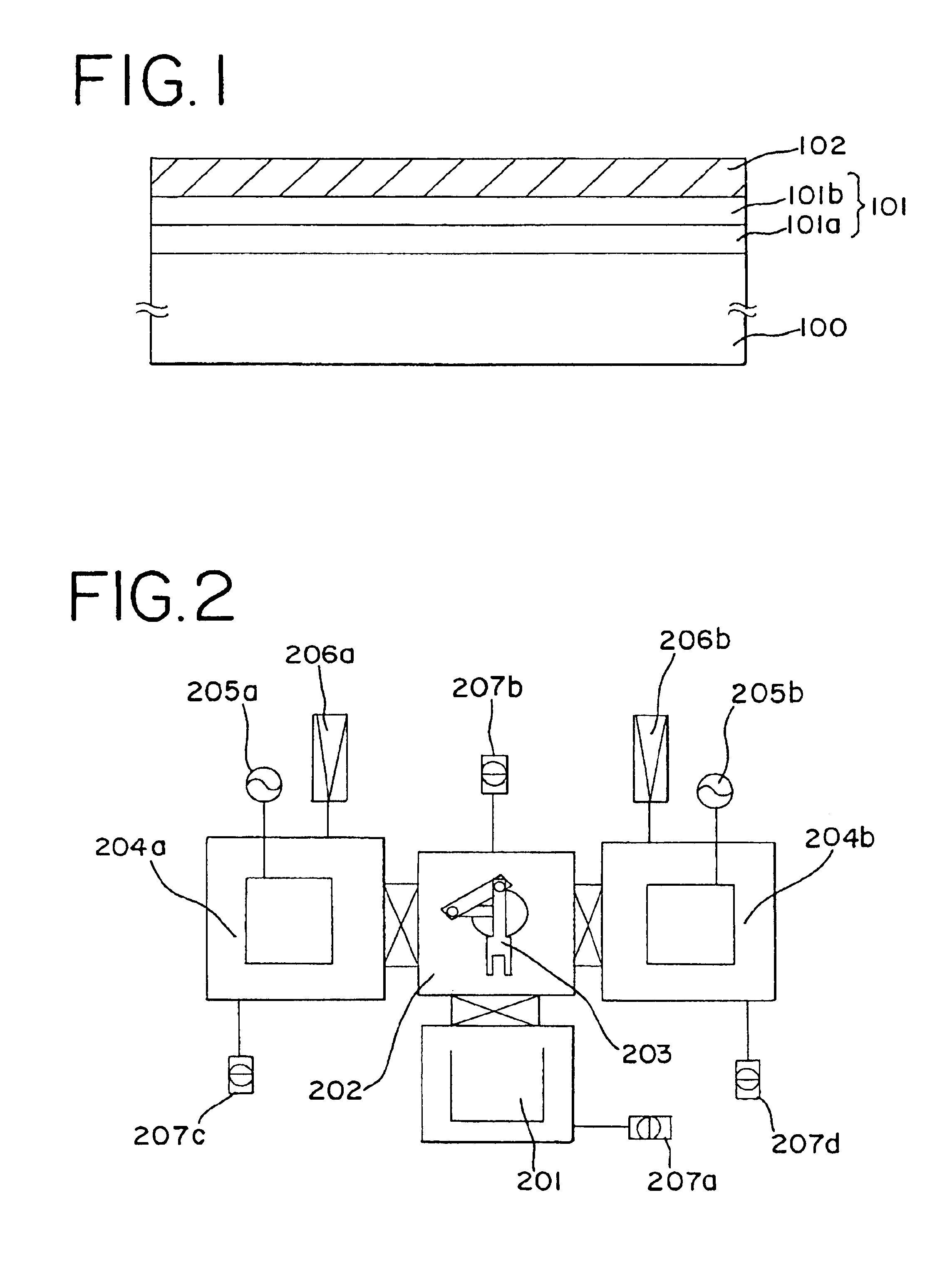
Embodiments of the present invention are described with reference to FIGS. 5A to 10. Here, a method of simultaneously manufacturing a pixel portion and TFTs (n-channel TFT and p-channel TFT) for forming a driver circuit provided in the vicinity of the pixel portion on the same substrate is explained in detail.

A glass substrate, a quartz substrate, a ceramic substrate and the like may be used for a substrate 500. Also, a silicon substrate, a metal substrate or a stainless substrate, formed with an insulating film on the surface, may be used. Further, a plastic substrate having heat resistance to a process temperature useable in this embodiment may also be used.

Next, as shown in FIG. 5A, a base film 501 formed of an insulating film such as a silicon oxide film, a silicon nitride film or a silicon oxide nitride film is formed on the substrate 500, and an amorphous semiconductor film 502 is sequentially formed on the base film 501. In this embodiment, a two layer structure is adopted fo...

embodiment 2

In this embodiment, a process of manufacturing an active matrix liquid crystal display device from the active matrix substrate manufactured in Embodiment 1 is described below. FIG. 11 is used for the explanation.

First, in accordance with Embodiment 1, after the active matrix substrate in the state of FIG. 8B is manufactured, an orientation film 601 is formed on the active matrix substrate of FIG. 8B, and a rubbing process is performed. Note that, in this embodiment, a columnar spacer 606 for maintaining an interval between substrates is formed at a desired position by patterning an organic resin film such as an acrylic resin film before the formation of the orientation film 601. Further, spherical spacers may be scattered onto the entire surface of the substrate instead of the columnar spacer.

Next, colored layers 604, 605 and a levelling film 607 are formed on an opposing substrate 603. The red-colored layer 604 and the blue-colored layer 605 are partially overlapped with each other...

embodiment 3

In this embodiment, a method of simultaneously manufacturing a pixel portion and TFTs (n-channel TFT and p-channel TFT) for forming a driver circuit in the vicinity of the pixel portion is explained with reference to FIGS. 12A to 14C.

First, as shown in FIG. 12A, on a substrate 1201 made of glass such as barium borosilicate glass or alumino borosilicate glass, typified by #7059 glass or #1737 glass of Corning Inc., preferably, gate electrodes 1202 to 1204, source wirings 1206, 1207 and a capacitor wiring 1205 for forming a storage capacitor of the pixel portion are formed from a conductive film containing one or a plurality of elements selected from the group consisting of molybdenum (Mo), tungsten (W) and tantalum (Ta). For example, an alloy of Mo and W is suitable from the viewpoint of low resistance and heat resistance. Further, the surface of the substrate may be oxidized using aluminum to form the gate electrode.

The gate electrode manufactured by a first photomask is formed with...


PUM


Abstract

At present, a forming process of a base film through an amorphous silicon film is conducted in respective film forming chambers in order to obtain satisfactory films. When continuous formation of the base film through the amorphous silicon film is performed in a single film forming chamber with the above film formation condition, crystallization is not sufficiently attained in a crystallization process. By forming the amorphous silicon film using silane gas diluted with hydrogen, crystallization is sufficiently attained in the crystallization process even with the continuous formation of the base film through the amorphous silicon film in the single film forming chamber.

Description

BACKGROUND OF THE INVENTION1. Field of the InventionThe present invention relates to a method of manufacturing a semiconductor device constituted of semiconductor elements typified by thin film transistors (hereinafter referred to as TFTs) using a crystalline semiconductor film formed on a substrate. Semiconductor devices manufactured in accordance with the present invention include not only elements such as a TFT and a MOS transistor but also a liquid crystal display device having a semiconductor circuit constituted of the above insulating gate type transistors (a microprocessor, a signal processing circuit, a high frequency circuit or the like), an EL (electro luminescence) display device, an EC (electro chromic) display device, an image sensor, and the like.2. Description of the Related ArtAt present, TFTs are used in integrated circuits as semiconductor elements using a semiconductor film, and particularly, as switching elements of an image display device. Further, TFTs in which...

Claims


Application Information

Patent Timeline
Patent Type & Authority Patents(United States)
IPC IPC(8): H01L21/70H01L21/02H01L29/66H01L27/12H01L21/336H01L29/786H01L21/84H01L21/20H01L21/205H01L21/77H01L27/32
CPCH01L27/12H01L27/1277H01L29/66757H01L29/66765H01L29/78675H01L29/78678H01L21/0237H01L21/02488H01L21/02672H01L21/02422H01L21/02491H01L21/02532H01L21/0262H01L27/1285H01L27/3244H10K59/12
Inventor ASAMI, TAKETOMIICHIJO, MITSUHIROTORIUMI, SATOSHI
Owner SEMICON ENERGY LAB CO LTD
Why Eureka
Try Eureka