Integrated circuit with a capacitor comprising an electrode
- Summary
- Abstract
- Description
- Claims
- Application Information
AI Technical Summary
Benefits of technology
Problems solved by technology
Method used
Image
Examples
second embodiment
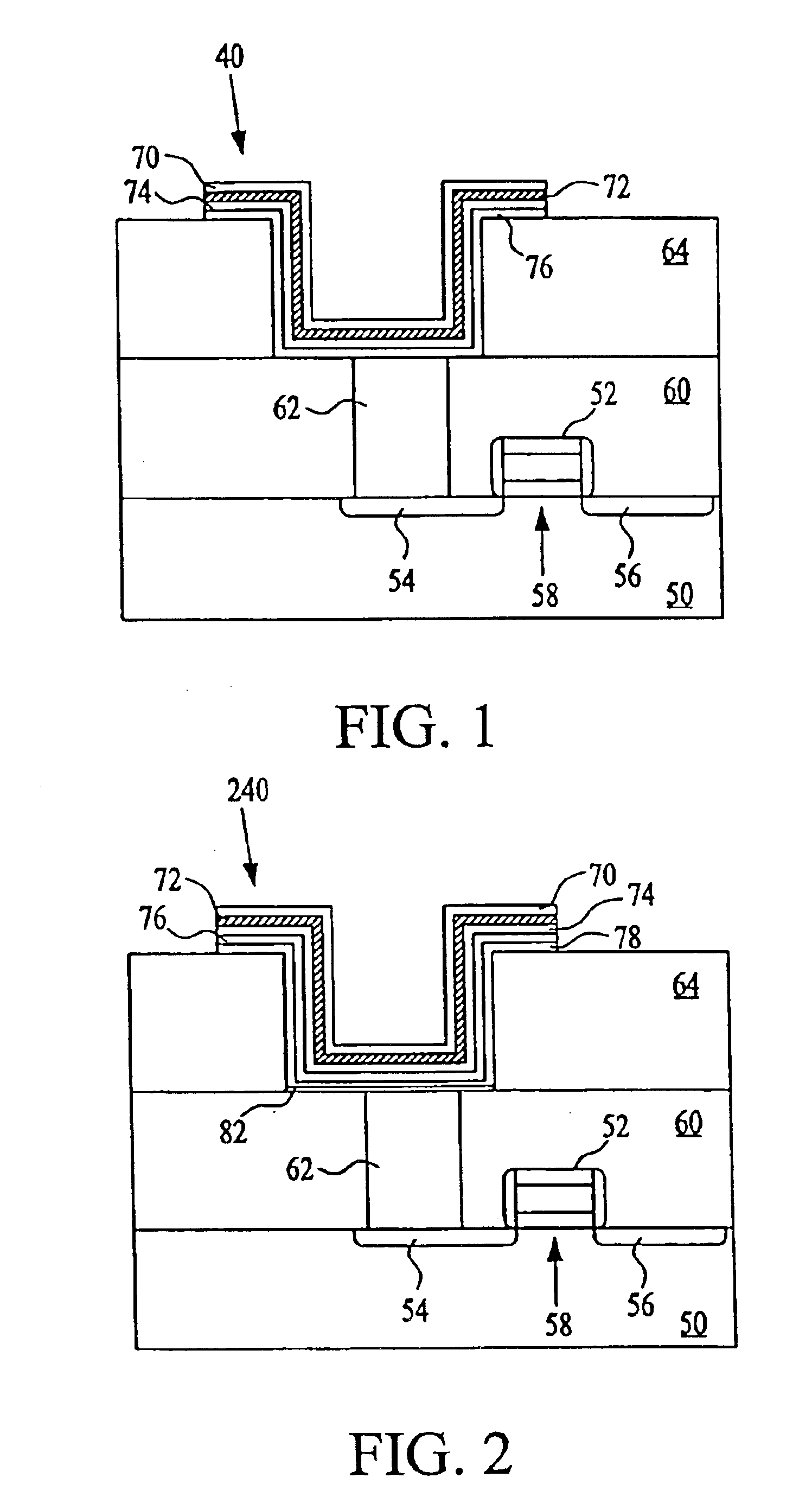
[0049]the capacitor 240 may be manufactured starting with the structure of FIG. 4 by a process depicted in FIGS. 9 through 14, and as described below. Referring to FIG. 9, a titanium layer 78 is formed on the surface of the protective layer 64 and in the trench 92 by means such as CVD, PVD, sputtering or evaporation. The titanium layer is formed to a thickness of about 60 to about 200 Angstroms, preferably about 60 to about 100 Angstroms. Next, as shown in FIG. 10, the platinum-rhodium layer 76 is formed by a suitable process such as CVD, as explained with reference to FIG. 5 above.
[0050]FIG. 11 depicts the next step in which the platinum layer 74 is formed on the surface of the platinum-rhodium layer 76. The dielectric layer 72 is then formed on the platinum-rhodium layer 76 by a sol-gel process, as shown in FIG. 12. During the heat treatment phase of the sol-gel process, a silicide layer 82 may be formed by an interaction between the titanium layer 78 and silicon of the oxide laye...
third embodiment
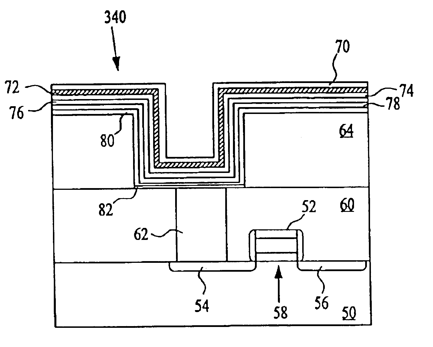
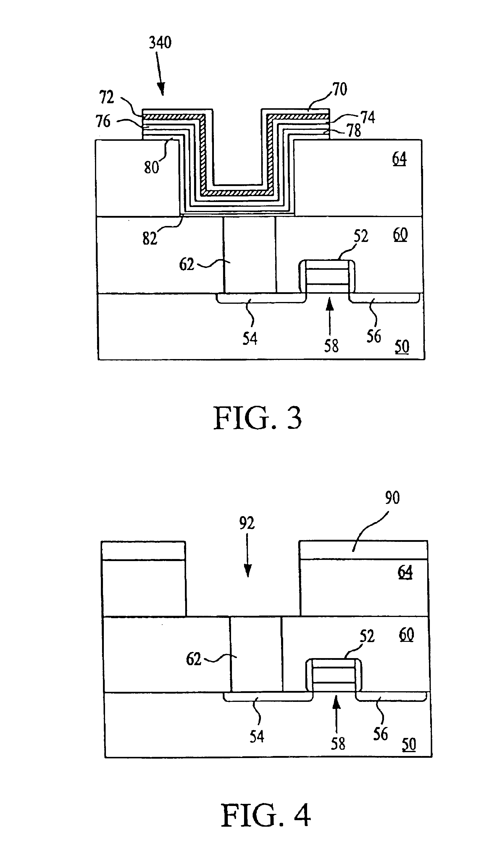
[0052]the capacitor 340 may be manufactured starting with the structure of FIG. 4 by a process depicted in FIGS. 15 through 21, and as described below. Referring to FIG. 15, a titanium nitride layer 80 is formed on the surface of the protective layer 64 and in the trench 92 by means such as CVD, PVD, sputtering or evaporation. The titanium nitride layer 80 is formed to a thickness of about 100 to about 200 Angstroms thick, preferably about 100 to about 150 Angstroms. Next, as shown in FIGS. 16 and 17, the titanium layer 78 and platinum-rhodium layer 76 are formed by suitable processes such as CVD, as explained with reference to FIGS. 9 and 10 above.
[0053]FIG. 18 depicts the next step in which the platinum layer 74 is formed on the surface of the platinum-rhodium layer 76. The dielectric layer 72 is then formed on the platinum-rhodium layer 76 by a sol-gel process, as shown in FIG. 19. During the heat treatment phase of the sol-gel process, a silicide layer 82 may be formed by an int...
PUM
 Abstract
Description
Claims
Application Information


