

Semiconductor device and manufacturing method thereof
a semiconductor and manufacturing method technology, applied in semiconductor devices, electrical devices, instruments, etc., can solve the problems of increasing the power consumption of the circuit, increasing the current flow, and relatively large junction leak curren
- Summary
- Abstract
- Description
- Claims
- Application Information
AI Technical Summary
Benefits of technology
Problems solved by technology
Method used
Image

Examples
embodiment 1
[0057]In this embodiment, a channel doping step is inserted in a process of forming a plurality of thin-film transistors on the same substrate. In particular, this embodiment is directed to a manufacturing method of thin-film transistors having superior circuit characteristics.
[0058]More specifically, this embodiment relates to a technique of improving the characteristics of the entire circuit or reduce the power consumption of the entire circuit by making Vth values of transistors different from one anther by controlling Vth's by use of a channel doping technique.
[0059]In this embodiment, a description will be made of part of a process to a channel doping step. Transistors can be completed by an ordinary method by using a silicon film produced by this embodiment.
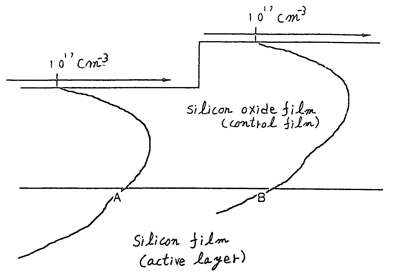
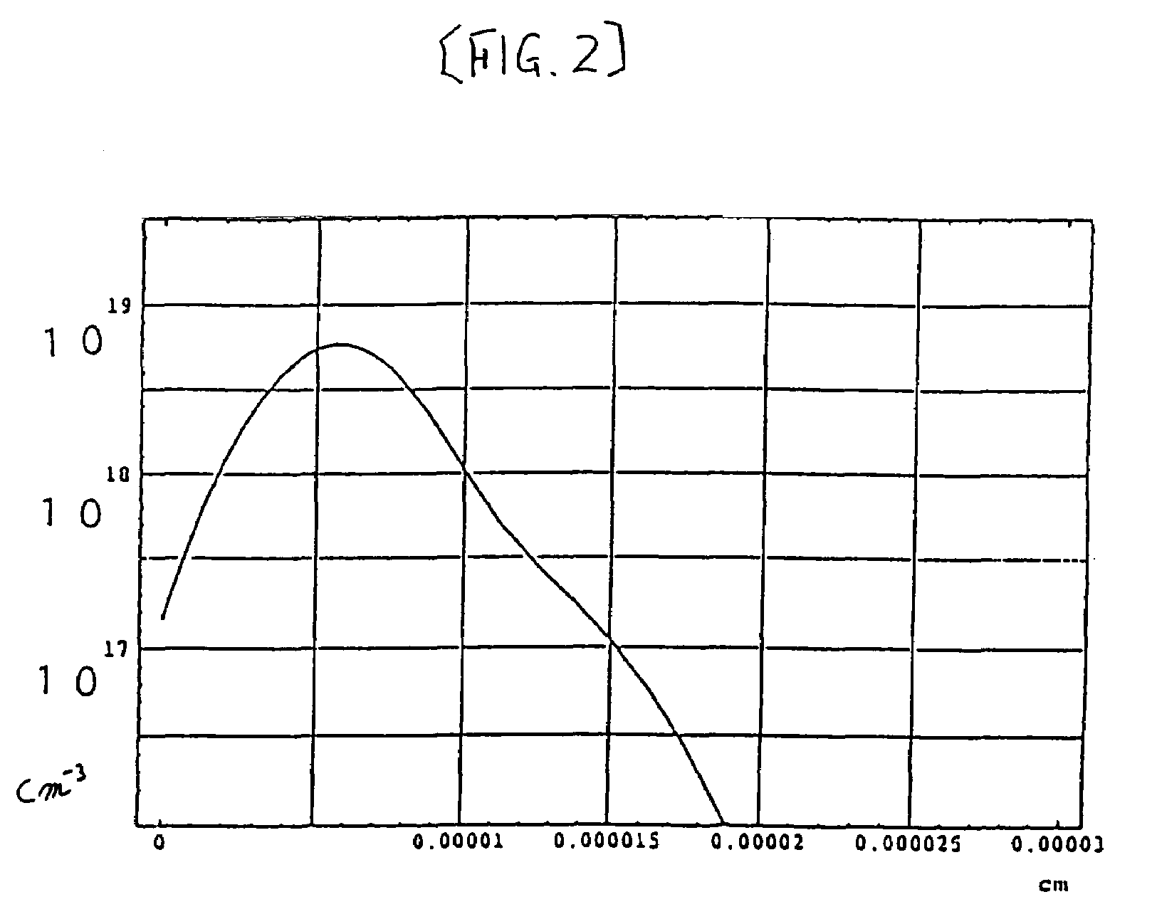
[0060]First, thin-film transistors in the midst of their manufacture, i.e., before being subjected to doping are prepared. Although the term “thin-film transistors” is used here, at this stage they merely include a 500-Å-th...
embodiment 2
[0087]A laser annealing step is inserted after the step of the first embodiment or performed instead of the thermal annealing, to further reduce lattice defects in the silicon oxide film, improve the crystallinity, and distribute the dopant uniformly over the entire substrate.
[0088]The silicon oxide film is removed by etching before the laser annealing.
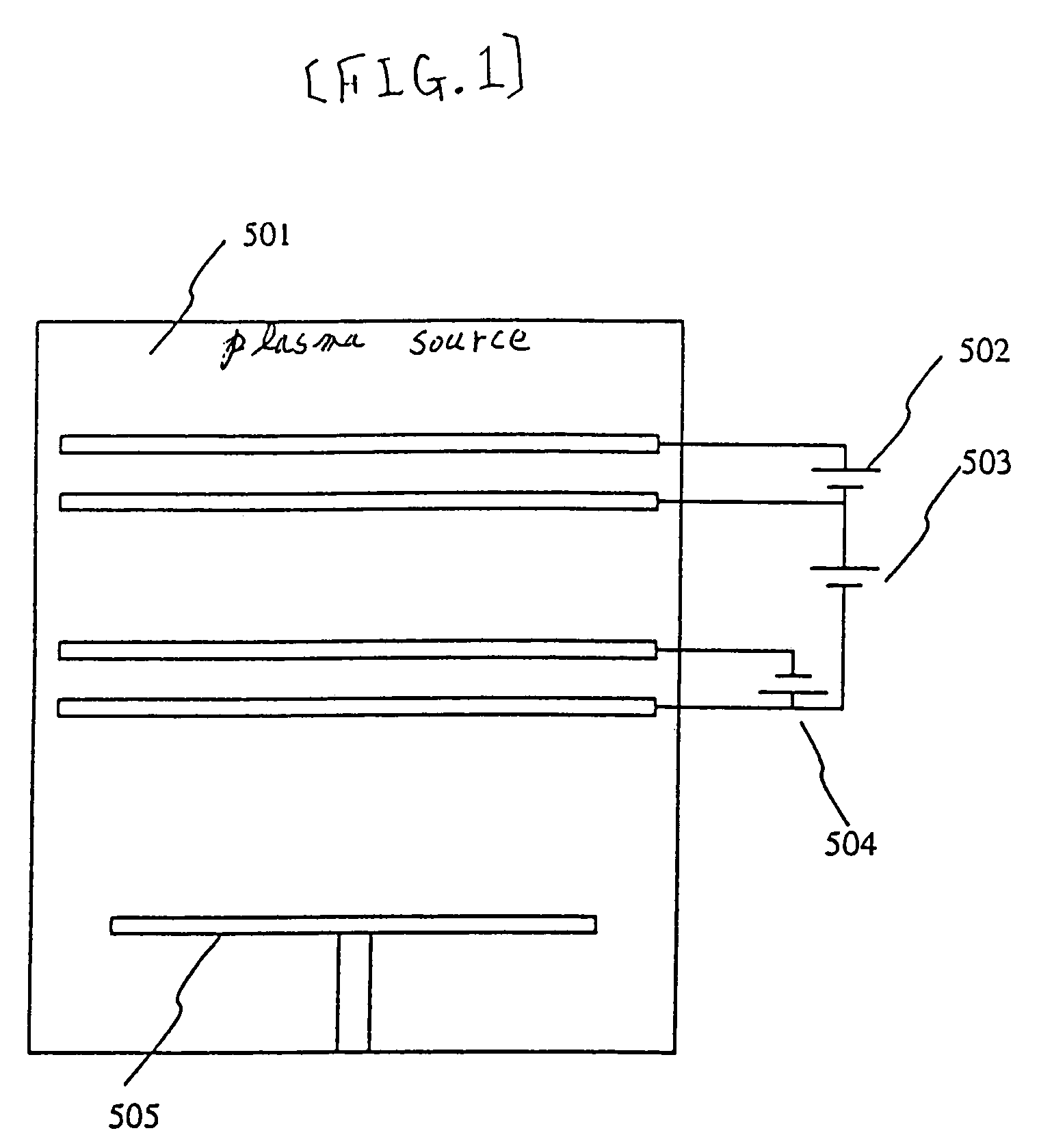
[0089]First, a description will be made of a laser apparatus. FIG. 3 shows the concept of a laser annealing apparatus used in this embodiment. KrF excimer laser light (wavelength: 248 nm; pulse width 25 ns) is emitted from an oscillator 2. Apparently other excimer lasers and other types of lasers may also be used.
[0090]The laser light emitted from the oscillator 2 is reflected by full-reflection mirrors 5 and 6, amplified by an amplifier 3, reflected by full-reflection mirrors 7 and 8, and introduced into an optics 4. Immediately before entering the optics 4, the laser beam has a rectangular shape of 3×2 cm2. The laser beam is shaped ...
embodiment 3
[0098]FIG. 6 shows a shift register circuit constituting a drive circuit of an active matrix display device which circuit can reduce leak current.
[0099]One output of the shift register is produced by one timing generation circuit and two voltage control circuit.
[0100]FFi−2 to FFi+2 are timing circuits, whose configuration is shown in FIG. 7. Each of the timing generation circuits FFi−2 to FFi+2 consists of one clocked inverter that is constituted of thin-film transistors having a low threshold voltage Vth and two inverters each constituted of thin-film transistors having a high threshold voltage Vth.
[0101]These thin-film transistors having different threshold voltages are ones that have been manufactured by the method of the first embodiment.
[0102]The timing generation circuits FFi−2 to FFi+2 generate scanning timing or image signal output timing of the active matrix display device.
[0103]In FIG. 7, clk is an operation clock signal for the timing generation circuit FFi, and *clk (log...
PUM
 Abstract
Description
Claims
Application Information