Method of forming semiconductor devices by microwave curing of low-k dielectric films

a technology of dielectric film and semiconductor device, which is applied in the direction of semiconductor/solid-state device manufacturing, basic electric elements, electric devices, etc., can solve the problems of reducing manufacturing throughput, increasing manufacturing costs, and difficult to meet the requirements of sub-micron-sized semiconductor device wiring, etc., to reduce thermal stress, reduce manufacturing throughput, and inhibit the formation of silanol bonds

Inactive Publication Date: 2009-07-07
GLOBALFOUNDRIES US INC
View PDF24 Cites 43 Cited by
  • Summary
  • Abstract
  • Description
  • Claims
  • Application Information

AI Technical Summary

Benefits of technology

[0035]This invention addresses the needs for an improved method of forming semiconductor devices with low-k inter-layer dielectrics for use in high-density, multi-level interconnection patterns. The adhesion of overlying layers on the ILD, such as barrier layers and etch-stop layers, is improved by the present invention. Also, an ILD is provided with densified surfaces that are not prone to degradation during etching and O2 ashing processes. The protection of the d...

Problems solved by technology

The escalating requirements for high density and performance associated with ultra large-scale integration (ULSI) semiconductor device wiring are difficult to satisfy in terms of providing sub-micron-sized, low resistance-capacitance (RC) metallization patterns.
As integration density increases and feature size decreases, in accordance with submicron design rules, the rejection rate due to integrated circuit speed delays significantly reduces manufacturing throughput and increases manufacturing costs.
However, as the size of openings for vias/contacts and trenches is scaled down to the sub-micron range, step coverage problems may result from the use of Al.
Poor step coverage causes high current density and enhanced electromigration.
For example, most W processes are complex and expensive.
Furthermore, W has a high resistivity, which decreases circuit speed.
Still a further problem is that W plugs are susceptible to void formation, and the interface with the metallization level usually results in high contact resistance.
The use of CVD for depositing Al is expensive and hot PVD Al deposition requires very high process temperatures incompatible with manufacturing integrated circuitry.
HSQ-type flowable oxides have been found to vulnerable to degradation during various fabrication steps, including plasma etching.
Thus, it was found that during subsequent barrier and metal deposition. e.g. titanium-nitride and tungsten, outgassing occurred thereby creating voids leading to incomplete electrical connections.
Further, the heat...

Method used


Image

  • Method of forming semiconductor devices by microwave curing of low-k dielectric films
  • Method of forming semiconductor devices by microwave curing of low-k dielectric films
  • Method of forming semiconductor devices by microwave curing of low-k dielectric films

Examples


Embodiment Construction

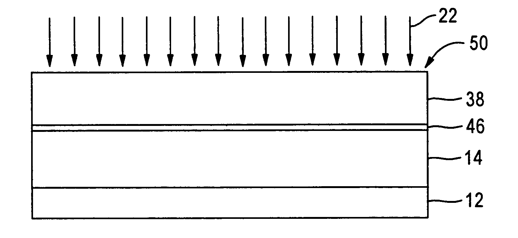
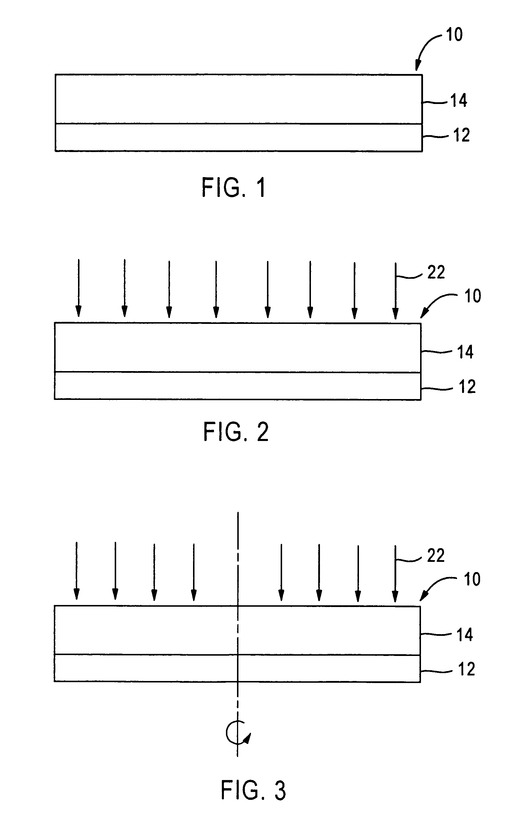
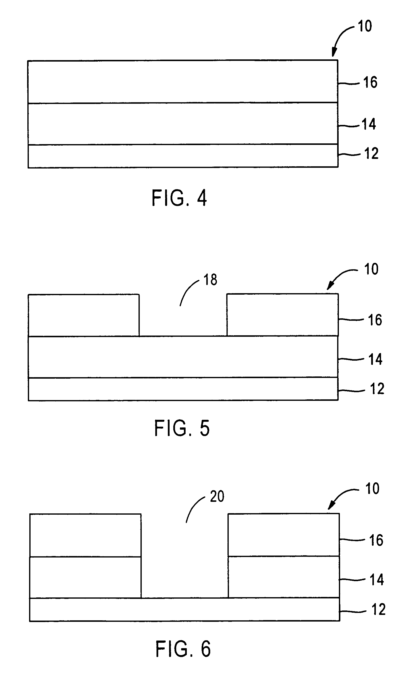
[0054]The present invention enables the production of semiconductor devices with improved performance and reduced feature sizes by exposing dielectric films to microwave radiation to cure the dielectric films. The microwave cured dielectric films provide a dielectric film surface which allows stronger adhesion of overlying layers, including barrier layers, etch-stop layers, and additional dielectric films. The microwave curing densifies the surface of the dielectric films, and makes the surface of the dielectric film more SiO2-like by causing silanol groups to crosslink at the dielectric surface. The lack of silanol bonds prevents the uptake of water and the resulting poisoned via phenomenon.

[0055]The term semiconductor devices, as used herein, is not to be limited to the specifically disclosed embodiments. Semiconductor devices, as used herein, include a wide variety of electronic devices including flip chips, flip chip package assemblies, transistors, capacitors, microprocessors, ...


PUM


Abstract

The invention provides a method of exposing low-k dielectric films to microwave radiation to cure the dielectric films. Microwave curing reduces the cure-time necessary to achieve the desired mechanical properties in the low-k films, thus decreasing the thermal exposure time for the NiSi transistor contacts. A lower thermal budget for interconnect fabrication is necessary to prevent damage to the NiSi transistor contacts and minimize thermal stressing of previously formed interconnect layers. Microwave-cured dielectric films also have higher mechanical strength and strong adhesion to overlying layers deposited during subsequent semiconductor device manufacturing steps.

Description

[0001]This application is a continuation of application Ser. No. 10 / 817,864, filed, Apr. 6, 2004 now abandoned.TECHNICAL FIELD[0002]The present invention relates to a method of manufacturing a semiconductor device exhibiting reduced capacitance loading. The present invention has particular applicability in manufacturing high-density, multi-level semiconductor devices comprising sub-micron dimensions and exhibiting high circuit speed.BACKGROUND OF THE INVENTION[0003]The escalating requirements for high density and performance associated with ultra large-scale integration (ULSI) semiconductor device wiring are difficult to satisfy in terms of providing sub-micron-sized, low resistance-capacitance (RC) metallization patterns. This is particularly applicable when the sub-micron-features, such as vias, contact areas, lines, trenches, and other shaped openings or recesses have high aspect ratios (depth-to-width) due to miniaturization.[0004]Conventional semiconductor devices typically com...

Claims


Application Information

Patent Timeline
IPC IPC(8): H01L21/4763
CPCH01L21/3105H01L21/31058H01L21/76825H01L21/3212H01L21/76813H01L21/32115
Inventor RYAN, E. TODDIACOPONI, JOHN A.
Owner GLOBALFOUNDRIES US INC
Why Eureka
Try Eureka