Rare earth-oxides, rare earth -nitrides, rare earth -phosphides and ternary alloys with silicon

a technology of rare earth oxides and ternary alloys, which is applied in the direction of lanthanide oxides/hydroxides, instruments, and semiconductor/solid-state device details, etc., can solve the problems of reliability degradation, dielectric breakdown, and difficult to replicate the high quality of si/sio/sub>2 interface in practically any other material system, and achieve high quality

Inactive Publication Date: 2011-03-08
IQE
View PDF36 Cites 6 Cited by
  • Summary
  • Abstract
  • Description
  • Claims
  • Application Information

AI Technical Summary

Benefits of technology

[0219]A further advantage of the present invention applied to SOI substrates using rare-earth metal oxide BOX layer is in the area of thermal dissipation. The thermal conductivity of SiO2 is approximately one hundred times lower than single crystal Si. It is well known that submicron transistor self-heating effects are problematic in ULSI FETs implemented on conventional SOI substrates. The present invention potentially alleviates this self-heating problem as the rare-earth metal oxides, nitrides and or phosphides exhibit substantially higher thermal conductivity than SiO2.
[0220]A further aspect of the present invention is a multiple layer periodic or aperiodic sequence or permutation of epitaxial growth of rare-earth oxide and or rare-earth nitride and or rare-earth phosphide and / or silicon and / or silicon-germanium.
[0221]In other embodiments of the present invention, the electronic transistor gate dielectric structures for an integrated circuit is disclosed. FIG. 11 illustrates one embodiment of an electronic transistor gate dielectric structure 1110 of the present invention. A first insulator and or dielectric layer 1118 is grown over a template layer and or buffer 1120. The dielectric layer 1118 is a single crystal rare-earth containing layer according to compositions of (1) through (6) above. A first semiconductor layer 1116 is deposited upon the first dielectric layer 1118. The semiconductor layer 1116 is preferably a single crystal semiconductor epitaxially deposited upon the single crystal dielectric layer1118 according to the present invention. The multi-layers are deposited over a substrate 1122. A second dielectric layer 1112 is deposited over the first semiconductor layer 1116. This basic layer sequence forms a single crystal semiconductor layer 1116 sandwiched by two dielectric layers. This basic structure is used to form a field effect transistor that is disposed upon an insulating substrate. Alternatively, the said structure forms a double gate field effect transistor. At least one of the dielectric layers 1112 and 1118 are made of the compositions of (1) through (6) above, as well as their various embodiments. The semiconductor layer 1116 is chosen preferentially as a single crystal silicon and or germanium layer. Each of the dielectric layers 1112 and or 1118 can be made of the single crystal compositions of (1) through (6) above, as well as their various embodiments.
[0222]Structures 1110 can have repeating units. By way of illustration, a third dielectric layer 1117 and a second semiconductor layer 1114 are deposited. If the second dielectric layer 1112 is made of the single crystal compositions of (1) through (6) above, then the second semiconductor layer can be single crystal in structure. The semiconductor layer 1114 is positioned between the second and third dielectric layers 1117 and 1112, respectively.
[0223]It will be appreciated that four or more dielectric layers can be provided. The third dielectric layer can be made of the compositions of (1) through (6) above. Therefore, it is clear that the use of single crystal compositions of (1) through (6) above, allows construction of single crystal multi-layers of semiconductor and insulator sequences, thereby allowing the entire structure to be single crystal.
[0224]Preferably, the substrate 1122 is chosen from single crystal silicon. The first semiconductor layer is chosen from single crystal silicon and or germanium. The first dielectric layer 1118 is chosen from substantially single crystal compositions of (1) through (6) above.

Problems solved by technology

The high quality of the Si / SiO2 interface is difficult to replicate in practically any other material system.
Unfortunately, fundamental physics problems at such small SiO2 thickness appear: (i) large quantum mechanical tunneling gate current; (ii) dielectric breakdown; and (iii) reliability degradation.
To date there does not exist a clear answer to this Si industry compatibility issue for optoelectronic materials.
However, to date all such alternative gate oxide candidates mentioned above fail in one or more areas of required device performance.
However, crystallinity in this case is not sufficient criterion for FET gate oxide suitability.
Unfortunately, the silicon / STO hetero-junction offset is almost entirely located in the valence band- and therefore is unsuited to Si-based ULSI FET devices.
Recent success of the ALD process for demonstration of ultrathin oxides mentioned above, unfortunately neglects specific problems related to practical ULSI device issues:
Central to the inadequacy of SiO2 as a viable ultrathin gate oxide is the presence of impurities, primarily those related to hydrogen, which are responsible for premature failure and low breakdown voltages in ULSI devices.
Therefore, it is unclear how hydride and chloride based precursor ALD solves this issue.
The issue of interface quality is typically not addressed, that is, the interfacial quality of bulk Si / high-k oxide.
Typically, the interfacial quality and / or defect density is inferior to that of the Si / SiO2 system and therefore FET channel and threshold voltage performance is compromised.
However, extensive CMP is still required to form a uniform flat active silicon layer surface.
Both forms of SOI, however, share the unfavorable properties that the Si / buried oxide interface is highly defective and is not usable as a lower gate dielectric layer for FET devices.
Secondly, both forms of SOI are presently costly to produce and it is this fact that hinders wider acceptance of SOI technology in present and future ULSI processes.
Thirdly, conventional SOI fabrication technologies are time consuming and physically require many serial processing and cleaning steps.
Fourthly, active Si layer thickness required for fully depleted SOI, typically less than or equal to 500 Angstroms, are extremely difficult to realize.
The disadvantage of this technique is stoichiometry of the target does not ensure stoichiometry of the resulting deposited thin film oxide.
A further disadvantage of this technique is that prolonged use of the single source EBE rare-earth oxide results in unfavorable rare-earth-to-oxygen ratio variation.
Yet another disadvantage of this technique is the lack of evaporant flux control by virtue of the EBE process.
Yet a further disadvantage of this technique is the introduction of charged species / defects that affect trapped oxide charge in an unfavorable manner.
A major disadvantage of aforementioned techniques, as discussed in U.S. Pat. No. 6,610,458, is the limitation to the type of rare-earth oxide that can be used.
If fact, cubic rare-earth crystals will have significant net charge defect due to the multiplicity of rare-earth oxide oxidation state-thereby rendering such oxides inapplicable to high performance FET devices.
The resultant films are similarly plagued by amorphous and or polycrystal RE-oxide phases.
Single crystal erbium-oxide films has not been demonstrated and or claimed as beneficial in prior art.
Similarly, single crystal rare-earth oxide and silicon multilayers have not been demonstrated.
In summary, using EBE of a chemically stoichiometric rare-earth oxide single target or rare-earth organic precursor, in general, does not ensure the correct deposited film stoichiometry.
This results in amorphous and or polycrystalline rare-earth oxide thin film.
Departure from stoichiometry in the film deposition structure results generally in strongly disordered structures.

Method used


Image

  • Rare earth-oxides, rare earth -nitrides, rare earth -phosphides and ternary alloys with silicon
  • Rare earth-oxides, rare earth -nitrides, rare earth -phosphides and ternary alloys with silicon
  • Rare earth-oxides, rare earth -nitrides, rare earth -phosphides and ternary alloys with silicon

Examples


example 1

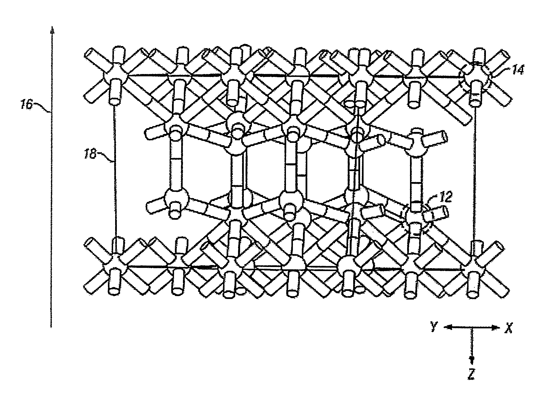
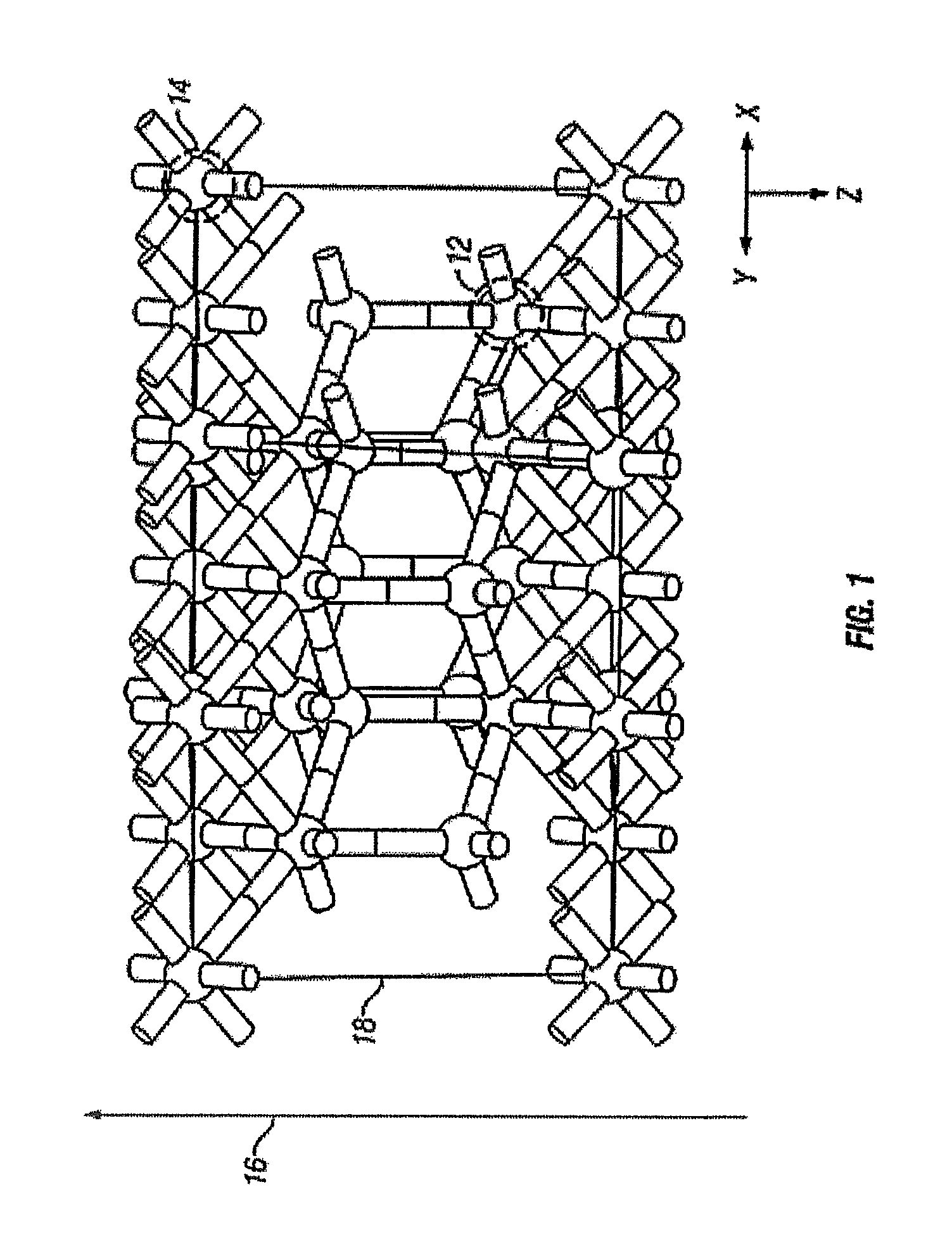
[0112]One structure for the epitaxial c-ErOx, representing the single crystal composition ErxOy, is shown in FIG. 1, where x and y are real positive numbers. In FIG. 1, the c-ErOx structure is a construction of a supercell with periodic boundary conditions and is generally denoted as 10. The rare-earth atoms are represented as dark spheres 12 and the lighter spheres represent oxygen atoms 14. The layer-by-layer growth direction 16 is co-incident with the crystal growth direction. A portion of one complete two-dimensional oxygen terminated layer is shown as 18.

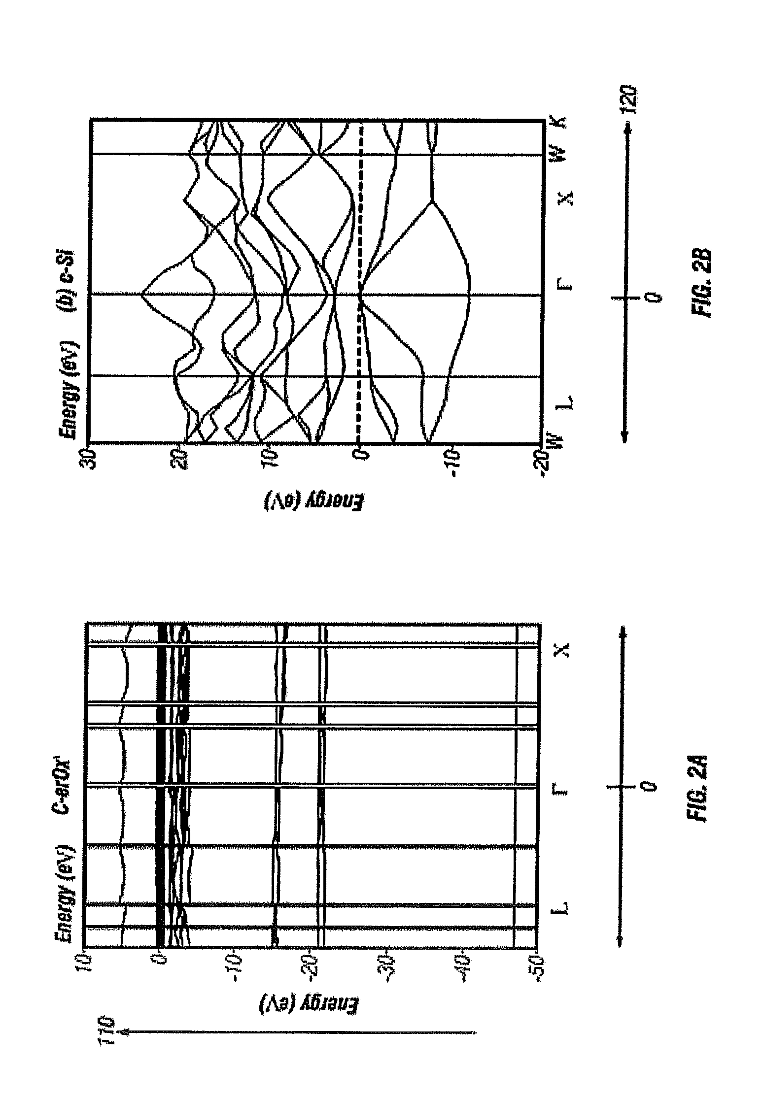
[0113]Using a density functional theory plane-wave psuedopotential method and self-consistent minimization, an energy-momentum calculation is performed. FIG. 2(a) illustrates energy E, denoted as 110, dispersion as a function of crystal momentum k, denoted as 120 of the single crystal rare-earth oxide ErxOy, of the present invention.

[0114]For comparison a bulk Si E-k curve is computed and shown in FIG. 2(b). c-ErOx has a quanti...

example 2

[0116]In one embodiment of the present invention, compositions are provided where nitrogen atoms with a very high affinity for accepting three electrons when forming RE compounds. That is, anions with N3− electronic states can form single crystal, polycrystal and amorphous rare-earth nitride compounds of the formula RE3+N3−. Conditions suitable for preparation RE—N compounds are for example using UHV environment suitable for deposition onto a substrate, an elemental RE source and source of atomic nitrogen (N) and or metastable excited molecular nitrogen (N2*) and or unexcited molecular nitrogen gas (N2).

[0117]Rare-earth nitride ErN binary compounds can have a greater disposition to crystallize in substantially cubic and or wurtzite structures. This crystal symmetry group is well suited to preferential epitaxial growth on diamond like crystal structures such as the Si(001)-oriented surface, or related misoriented surfaces. In one specific embodiment of the present invention, RE—N com...

example 3

[0118]In one embodiment, substantially single crystal, rare-earth phosphide compositions are provided. Under suitable conditions phosphorous forms strong ionic RE—P bonds. The phosphorous atoms or molecules have a very high affinity for accepting three electrons when forming RE compounds. That is, anions with P3− electronic states can form single crystal, polycrystal and amorphous rare-earth phosphide compounds of the formula RE3+P3−. Conditions suitable for preparation RE—P compounds are, for example, using UHV environment suitable for deposition onto a substrate, an elemental RE source, a source of atomic phosphorous (P), molecular phosphorous (P2 and or P4), sublimation of phosphide compounds, and the like.

[0119]Rare-earth nitride ErP binary compounds can have a greater disposition to crystallize in substantially cubic and or wurtzite structures. This crystal symmetry group is well suited to preferential epitaxial growth on diamond like crystal structures such as the Si(001)-orie...


PUM

PropertyMeasurementUnit
thicknessaaaaaaaaaa
wavelengthsaaaaaaaaaa
thicknessaaaaaaaaaa

Abstract

Atomic layer epitaxy (ALE) is applied to the fabrication of new forms of rare-earth oxides, rare-earth nitrides and rare-earth phosphides. Further, ternary compounds composed of binary (rare-earth oxides, rare-earth nitrides and rare-earth phosphides) mixed with silicon and or germanium to form compound semiconductors of the formula RE-(O, N, P)—(Si,Ge) are also disclosed, where RE=at least one selection from group of rare-earth metals, O=oxygen, N=nitrogen, P=phosphorus, Si=silicon and Ge=germanium. The presented ALE growth technique and material system can be applied to silicon electronics, opto-electronic, magneto-electronics and magneto-optics devices.

Description

CROSS-REFERENCE TO RELATED APPLICATIONS[0001]This application claims benefit of U.S. provisional patent application Ser. No. 60 / 533,378 filed on 29 Dec. 2003, and is also a continuation-in-a-part of U.S. Ser. No. 10 / 825,974 filed Apr. 16, 2004, now U.S. Pat. No. 6,858,864 which is a continuation of U.S. Ser. No. 10 / 666,897 filed Sep. 17, 2003, now U.S. Pat. No. 7,023,011 which is a divisional of 09 / 924,392 filed Aug. 7, 2001, now U.S. Pat. No. 6,734,453 which claims the benefit of U.S. Ser. No. 60 / 223,874 filed Aug. 8, 2000, all of which applications are herein incorporated by reference.BACKGROUND OF THE INVENTION[0002]1. Field of the Invention[0003]The invention relates generally to compositions, structures and devices for silicon-on-insulator (SOI) compositions, devices and applications, and more particularly to compositions, structures and devices utilizing substantially single crystal compositions for SOI compositions, devices and applications.[0004]2. Description of the Related...

Claims


Application Information

Patent Timeline
Patent Type & Authority Patents(United States)
IPC IPC(8): H01L31/0264B32B9/04C01F17/224C01F17/241C30B23/00C30B25/00C30B28/12C30B28/14C30B29/16H01L21/314H01L21/316H01L21/44H01L23/58H01L29/06H01L29/26H01L29/51
CPCB82Y20/00G02B6/1225G02B6/125H01L21/3141H01L27/15H01L29/26H01L29/51H01L33/34H01S5/18341H01L21/3143H01L21/31645H01S3/0604H01S3/0627H01S3/1603H01S3/1628H01S5/0261H01S5/18369H01S2301/173B32B9/04C01B25/08C30B29/38C01P2002/85C01B21/0602B32B9/005B32B2307/702B32B2307/704B32B2307/732B32B2457/00C30B25/02C30B29/14C30B29/22C01F17/224C01F17/241H01L21/02156H01L21/02192H01L21/0228C30B29/16
Inventor ATANACKOVIC, PETAR B.
Owner IQE
Why Eureka
Try Eureka