Method for preparation of one-dimensional silicon nanostructure

A silicon nanometer and nanoparticle technology, which is applied in the field of preparation of one-dimensional silicon nanostructures, can solve the problems that nanomaterials are difficult to meet the needs of application occasions, and achieve the advantages of device fabrication and assembly, compatible processing technology, and good repeatability Effect

Inactive Publication Date: 2008-02-06
SUN YAT SEN UNIV
View PDF0 Cites 27 Cited by
  • Summary
  • Abstract
  • Description
  • Claims
  • Application Information

AI Technical Summary

Problems solved by technology

However, the nanomaterials formed by these existing preparation methods are difficult to meet the requirements of the aforementioned applications.

Method used


Image

  • Method for preparation of one-dimensional silicon nanostructure
  • Method for preparation of one-dimensional silicon nanostructure
  • Method for preparation of one-dimensional silicon nanostructure

Examples


preparation example Construction

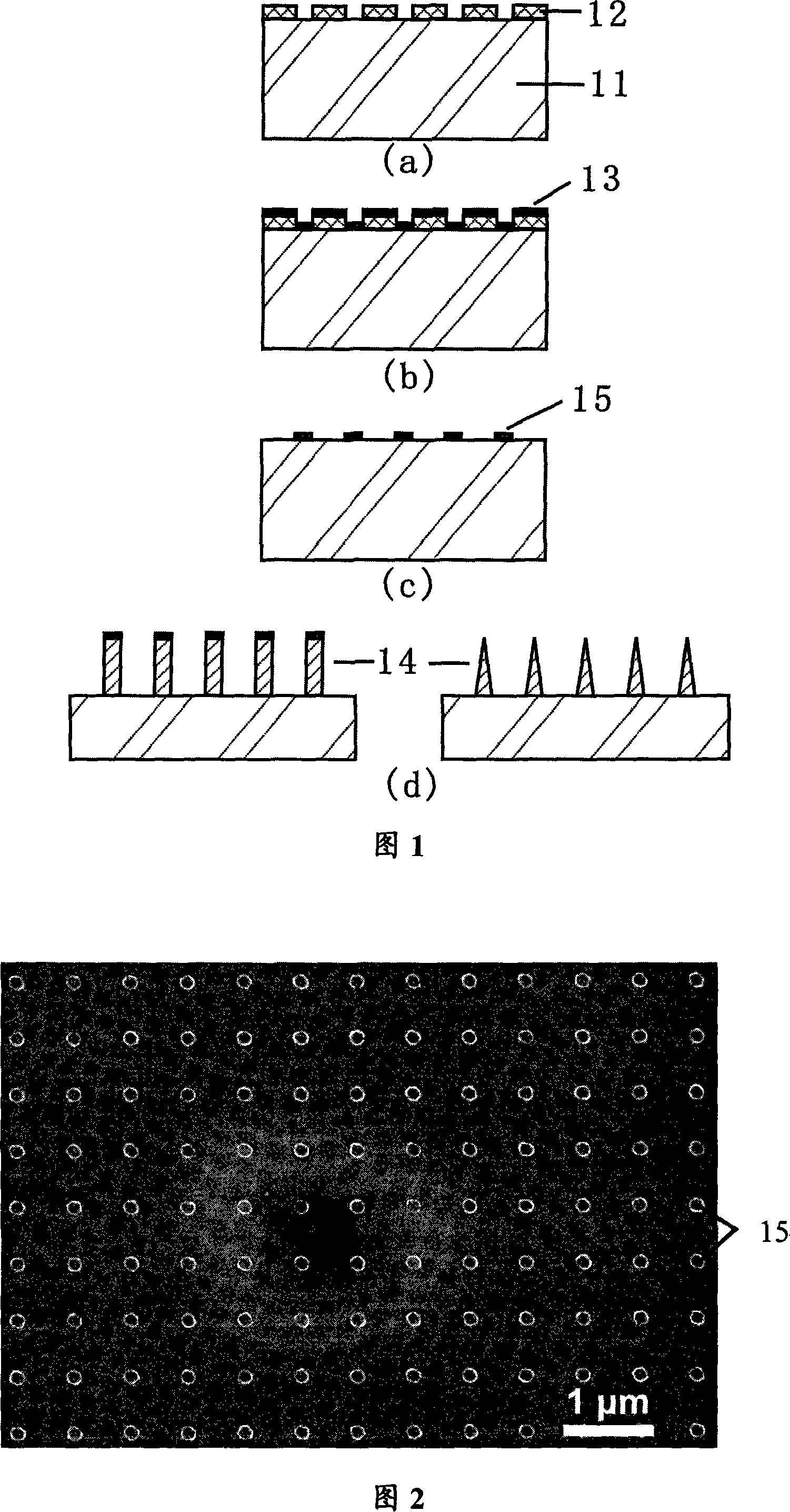
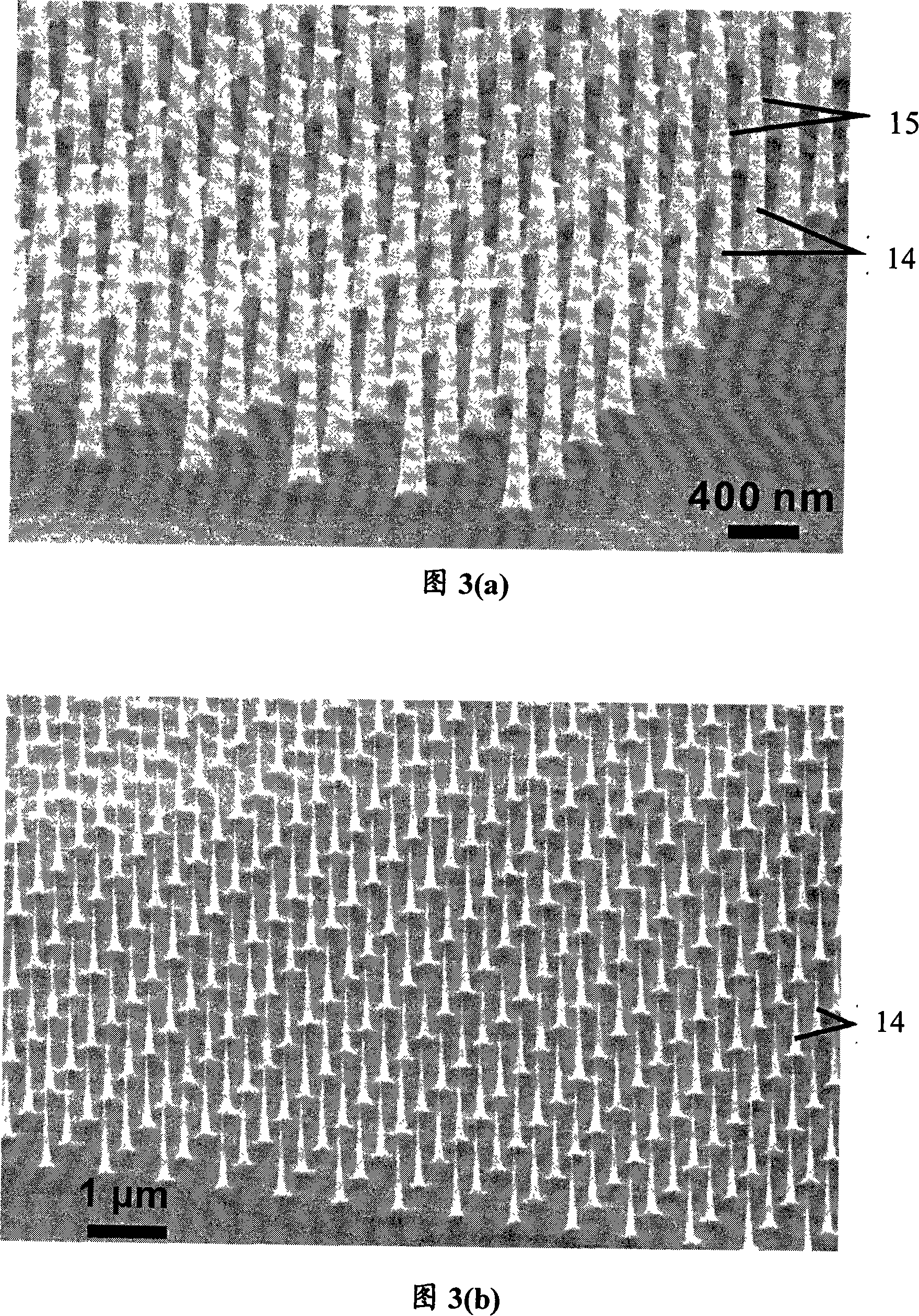
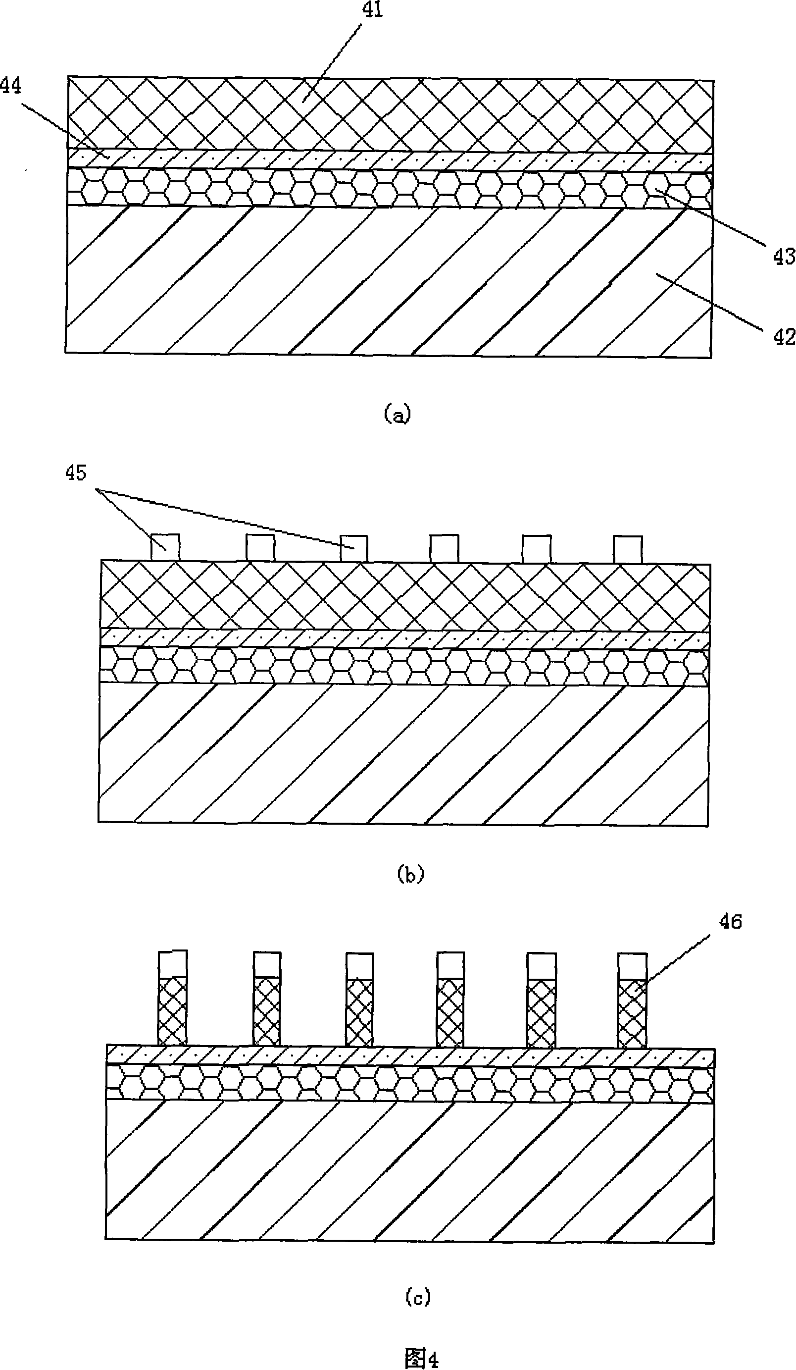
[0028] When the preparation and dispersion method of nanoparticles is used to obtain a nanoparticle mask, the process steps are as follows: first deposit a layer of metal film on the surface of the base material; then heat-treat the metal film to obtain a metal nanoparticle mask on the surface of the base material ; Finally, the base material is etched by plasma etching technology.

[0029] The present invention will be described in further detail below with different nanoparticle mask forming methods in conjunction with the accompanying drawings:

Embodiment 1

[0031] In this embodiment, electron beam lithography technology is used to form a nanoparticle mask, and single crystal silicon is used as the base material. The specific process steps are as follows:

[0032] 1. Use n-type high-conductivity single crystal silicon with crystal orientation (resistivity 2.4~3.7×10 -3 Ω·cm)11 as the substrate.

[0033] 2. Use a KW-4AH hot plate to bake the silicon substrate at a temperature of 180°C before gluing for 30 minutes.

[0034] 3. Using a Karl Suss RC8 coating machine, evenly spin-coat a layer of electron beam photoresist PMMA (950K C4) 12 on the surface of the baked silicon substrate, the coating speed is 3000rpm, and the acceleration is 10000rpm / s, The time is 30 seconds, and the glue thickness is 380nm.

[0035] 4. Use the KW-4AH hot plate to pre-bake the coated sample, the baking temperature is 180°C, and the baking time is 90s.

[0036] 5. Using the Raith E-line electron beam exposure system, on the PMMA-coated sample, expose t...

Embodiment 2

[0046]In this embodiment, the preparation and dispersion method of nanoparticles is used to obtain a nanoparticle mask, and the substrate deposited with an amorphous silicon film is used as the base material. The specific process steps are as follows:

[0047] 1. as shown in Figure 4 (a), deposit one layer of 0.5 μm silicon dioxide (SiO 2 ) layer 43 and a 0.2 μm metal chromium (Cr) layer 44 as a substrate, wherein the metal chromium (Cr) layer 44 is on top of the silicon dioxide layer 43 .

[0048] 2. Place the substrate in a plasma-enhanced chemical vapor deposition system (PECVD) to deposit the amorphous silicon film 41 , as shown in FIG. 4( a ). where the reaction gas is SiH at 400 sccm 4 (5%) / Ar(95%), the radio frequency source (RF) power is 40W, the reaction pressure is 60Pa, the deposition time is 60 minutes, and the corresponding film thickness is about 1.2 μm.

[0049] 3. Deposit a layer of gold film with a thickness of several nanometers by DC sputtering on the surf...


PUM

PropertyMeasurementUnit
electrical resistivityaaaaaaaaaa
diameteraaaaaaaaaa
heightaaaaaaaaaa

Abstract

The invention discloses a method for preparing one-dimensional silicon nanostructure. The order of the processing steps adopted by the invention is as follows: (A) nanometer particle mould is prepared on the surface of backing material; (B) etching of the backing material is completed by use of plasma etching technology. The step (A) includes the following procedures: (i) the surface of backing material is coated with one layer of photoresist through spin coating at first, and then micropores are formed at the surface of backing material through adopting electronic photoetching technique; (ii) one layer of mask film is deposited on the surface of backing material; (iii) photoresist peeling-off of the surface of backing material deposited with the mask film is completed so as to form the nanometer particle mask at the micropores of procedure (i). In addition, step (A) can also be as follows: one layer of metallic film is firstly deposited on the surface of backing material and then heat treatment of the metallic film is completed to obtain metallic nanometer particle mask on the surface of backing material. The silicon nano wire / tip prepared by the invention is characterized in erection, order and controllable position and diameter etc., thereby being particularly favorable to manufacture and assembly of device.

Description

technical field [0001] The invention relates to the technical field of design and manufacture of nanomaterials, in particular to a method for preparing a one-dimensional silicon nanostructure. Background technique [0002] Quasi-one-dimensional nanomaterials, such as carbon nanotubes, silicon nanowires / tips, and silicon carbide nanowires, have nanoscale effects such as quantum confinement, Coulomb blockade, quantum tunneling, and tip surface field emission enhancement, making them ideal for photoelectric applications. Performance reflects different characteristics from bulk materials. Among these materials, silicon nanowires / tips have attracted much attention due to their unique electron transport and field electron emission properties, as well as their compatibility with traditional semiconductor integrated circuit processes. At present, there are mainly the following methods for preparing silicon nanowires / tips: (1) laser ablation (laser ablation), (2) thermal evaporation...

Claims


Application Information

Patent Timeline
Patent Type & Authority Applications(China)
IPC IPC(8): B82B3/00
Inventor 许宁生佘峻聪何浩姚日晖邓少芝陈军
Owner SUN YAT SEN UNIV
Why Eureka
Try Eureka