Method of processing semi-conductor industrial waste water

A technology for industrial wastewater and treatment methods, which is applied in osmosis/dialysis water/sewage treatment, chemical instruments and methods, semi-permeable membrane separation, etc. It can solve the problems of easy pollution of filter structures, unstable effluent quality, and high energy consumption in operation. Achieve the effects of easy automatic control, harmless wastewater, and reliable system operation

Inactive Publication Date: 2008-08-06
无锡凝洋环保科技有限公司
View PDF5 Cites 5 Cited by
  • Summary
  • Abstract
  • Description
  • Claims
  • Application Information

AI Technical Summary

Problems solved by technology

Disclosed in the patent application entitled "Dehydration Treatment Method of Inorganic Sludge Formed by Dehydration Treatment of Colored Glass Shell Grinding Water", the application number is ZL200610013764, the publication number is CN / 101007697, and the publication date is August 1, 2007 A dehydration treatment method for inorganic sludge formed by dehydration treatment of colored glass shell grinding wastewater. It first uses polyacrylamide to flocculate and concentrate the sludge, and then enters the bag filter press for pressure filtration, but the treatment process Chemical agents need to be added in the medium, which will cause secondary pollution to the permeate, and the operating cost is high
In the patent application entitled "A Fiber Ultrafiltration Method and Equipment", the application number is ZL200510041374, the publication number is CN1743055, and the publication date is March 8, 2006, a patent application using fiber prefiltration steps and ultrafiltration treatment is disclosed. The method of grinding wastewater, which first passes the grinding wastewater through the fiber microfiltration part of 1-10 microns, and then enters the roll-type ultrafiltration membrane with a cut-off pore size of 0.01-0.03 microns for filtration by means of pressurization. The filter structure is easy to be polluted, so frequent backwashing is required, and the water production rate of the whole process is less than 85%
[0008] The above-mentioned water treatment methods have the problems of large and complex structure of treatment facilities, large floor area, very expensive investment and operation costs, and the treatment process usually requires adding a variety of chemicals to achieve metal ion precipitation and solid particle flocculation precipitation, thereby A large amount of harmful sludge is produced during the treatment process, and organic pollutants are filtered through reverse osmosis, which has disadvantages such as complicated operation, unstable effluent quality, unrecyclable effluent, and high energy consumption in operation.

Method used


Image

  • Method of processing semi-conductor industrial waste water

Examples


Embodiment 1

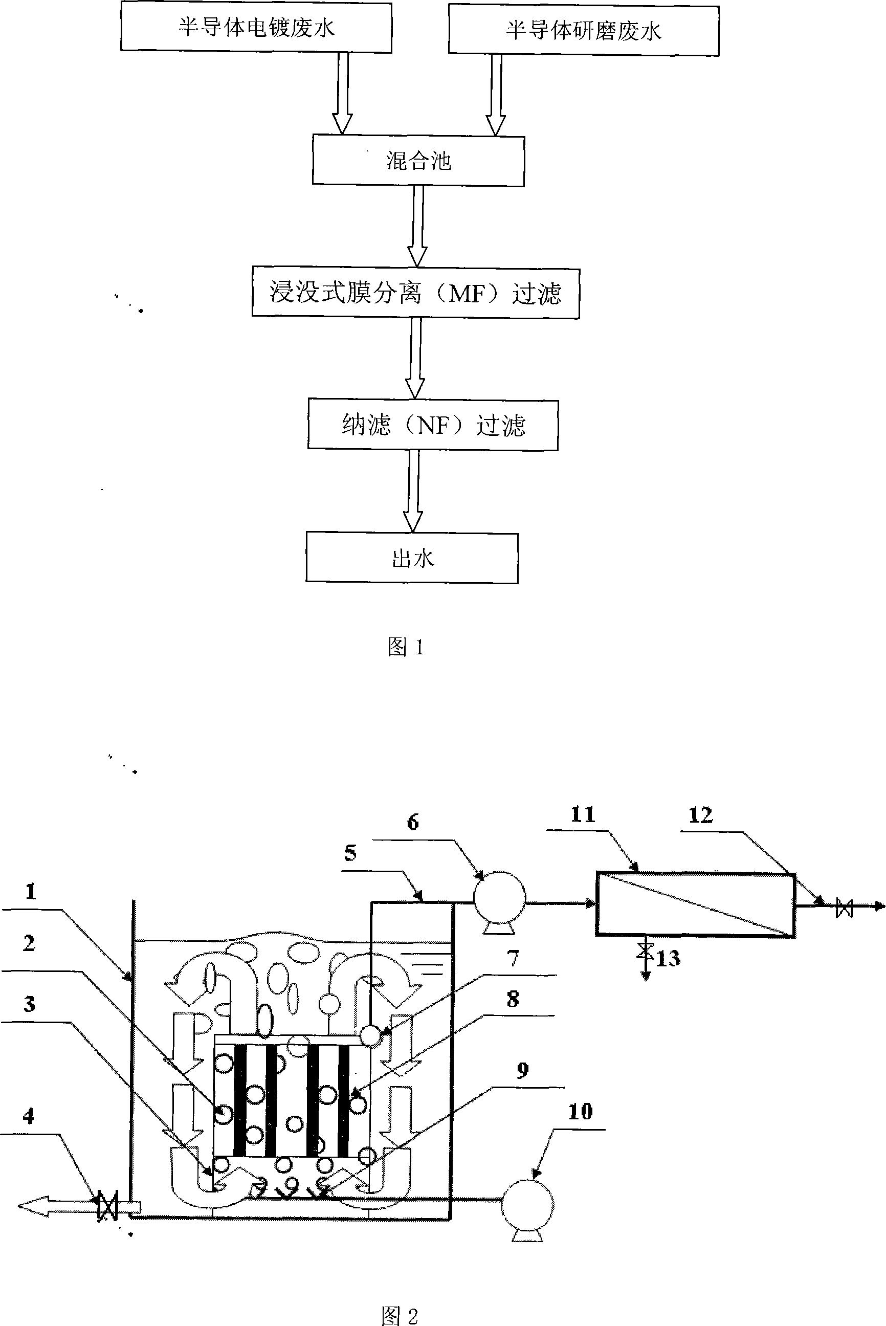
[0025]As shown in the process flow in Figure 1, the silicon wafer electroplating wastewater produced by a microelectronics company's integrated circuit and the grinding wastewater of the packaging shell are discharged into the mixing pool to become mixed wastewater. The water quality is shown in Table 2. The submerged flat-plate membrane filtration device designed and manufactured by Wuxi Ningyang Environmental Protection Technology Co., Ltd. has a Chinese patent application number of 200720035758.4, and its structure diagram is shown in Figure 2. The filter membrane used in this equipment is a flat submerged organic polymer material microfiltration membrane (MF), its filter pores are between 0.04 and 0.5 μm, and the operating pressure is less than 20KPa, which can effectively remove suspended solids, The micelles, particles and most of the organic impurities, the water quality of the above-mentioned semiconductor processing mixed wastewater after being filtered by the submerge...

Embodiment 2

[0034] An electronic technology company specializing in the development and production of semiconductor discrete devices. The water quality of the grinding wastewater and discrete device electroplating wastewater produced by its semiconductor manufacturing is listed in Table 3 after being discharged into the mixing tank. The packaging shell of the semiconductor discrete device is first electroplated with copper and then electroplated with nickel. The above-mentioned semiconductor processing mixed wastewater in the mixing tank is pumped into the submerged membrane filter device for treatment, and the filtered water quality is shown in Table 3 ("-" in the table means that it cannot be detected, and its value is close to zero). The permeate enters the nanofiltration device for further filtration treatment, and the finally filtered water can be reused directly. The water quality is shown in Table 3.

[0035] Table 3 The water quality of the above-mentioned semiconductor processing...


PUM

PropertyMeasurementUnit
electrical resistivityaaaaaaaaaa
pore sizeaaaaaaaaaa
retention rateaaaaaaaaaa

Abstract

The invention relates to a process method for semiconductor industry wastewater. The invention is principally used for treating and reusing of the waste water generated in the reducing process of the semiconductor production enterprises. The invention is characterized in that the following steps are included in the process: (1) the electroplating water and the grinding water generated in the production process of the semiconductor elements are mixed together for forming a mixed waste water; (2) the mixed waste water in step (1) is pumped into a submerged membrane filtering device for filtering; (3) the filtered water in step (3) is pumped into a nanofiltration membrane filtering device for filtering and the filtered water filtered through the nanofiltration membrane filtering device can be directly reused. In the invention, filtering treatment is carried out for the mixed waste water generated in a semiconductor process through the submerged membrane filtering device and the nanofiltration membrane filtering device, the recycled water source rate is bigger than 85 percent. The recycled water has a stable quality which completely arrives or is better than the national standard. The whole treatment process has no chemical medicine; therefore, no detrimental sludge is produced. The processing method for semiconductor industry wastewater has the advantages of low operation cost and non-detrimental compressed sludge as well as easy treatment.

Description

technical field [0001] The invention relates to a water treatment method, in particular to a treatment method for semiconductor industrial wastewater, more precisely, to a treatment method for silicon wafer cutting and grinding wastewater and parts electroplating wastewater generated during the production of semiconductor devices. Background technique [0002] The semiconductor industry is an industry that is very dependent on water resources and is also a high water-consuming industry. Especially in the case of limited water resources, water restrictions and water shortages have put enormous pressure on the operations of semiconductor manufacturers. Therefore, the research and practice of water conservation in semiconductor manufacturing enterprises will help improve water efficiency and reduce water costs. At present, water conservation, reuse of reclaimed water, and recycling of waste water have become important measures for the semiconductor industry to deal with the wat...

Claims


Application Information

Patent Timeline
Patent Type & Authority Applications(China)
IPC IPC(8): C02F1/44B01D61/18B01D69/12B01D71/42B01D71/56
Inventor 王毅刚王昕彤王前
Owner 无锡凝洋环保科技有限公司
Why Eureka
Try Eureka