

Method for processing GaN epitaxial substrate
A processing method and substrate technology, which are applied in the manufacturing of electrical components, circuits, semiconductor/solid-state devices, etc., can solve the problems of easy introduction of impurities, high production cost, increased stress, etc. The effect of reducing the processing cost
- Summary
- Abstract
- Description
- Claims
- Application Information
AI Technical Summary
Problems solved by technology
Method used
Image

Examples
Embodiment 1
[0029] Utilize the method of the present invention to prepare SiC substrate, comprise the following steps:
[0030] (1) Grinding the SiC single crystal rod cut by the wire saw to remove the knife marks on the wafer:
[0031] a. Use silicon carbide powder with a particle size of 20 μm, and mix it with water and suspending agent at a weight ratio of 1:1:0.1 to form a non-toxic grinding liquid with good fluidity, good suspending ability, and the suspending agent used is glycerin;
[0032] b Use a grinding machine to use a cast iron grinding disc and use the prepared grinding liquid to grind the SiC sheet in one or more stages until the knife marks on the wafer are removed, and the pressure on the wafer is 30g / cm 2 ;
[0033] (2) Carry out chemical mechanical polishing to the ground SiC wafer until the damaged layer of grinding is completely removed:
[0034] aUsing diamond micropowder with a particle size of 5 μm, the micropowder, water, dispersant and suspending agent are prep...
Embodiment 2
[0040] Adopt chemical mechanical polishing method of the present invention to prepare sapphire substrate, specific polishing method and polishing result are identical with embodiment 1, difference is, during grinding and chemical mechanical polishing, the pressure on the control wafer is 300g / cm 2, the suspending agent that adopts is ethylene glycol. When grinding, use boron carbide powder with a particle size of 40 μm, and the weight ratio of the powder, water and suspending agent in the grinding liquid is 1:100:200; during chemical mechanical polishing, use silicon carbide powder with a particle size of 10 μm, and the polishing disc uses a tin plate , the dispersant used is triethanolamine, and the weight ratio of micropowder, water, dispersant and suspending agent in the polishing liquid is 1:100:5:100. After chemical mechanical polishing, the annealing temperature of the wafer is 1500° C., and the holding time is 20 hours.
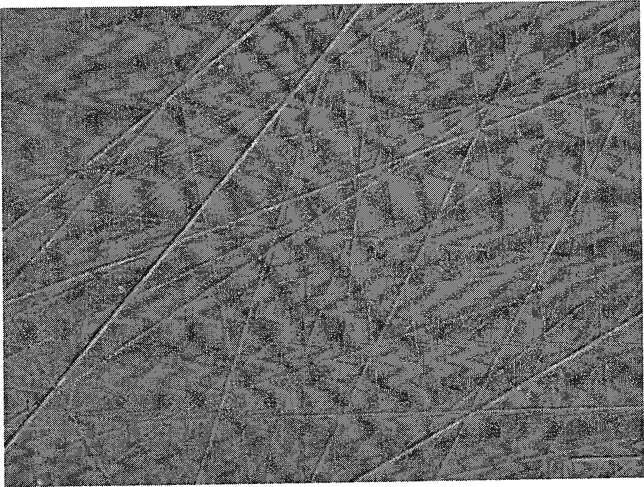
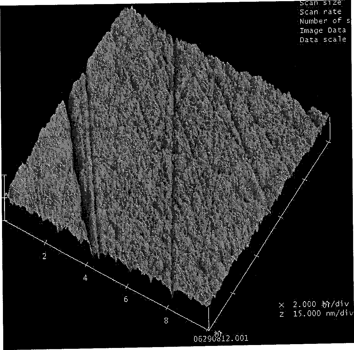
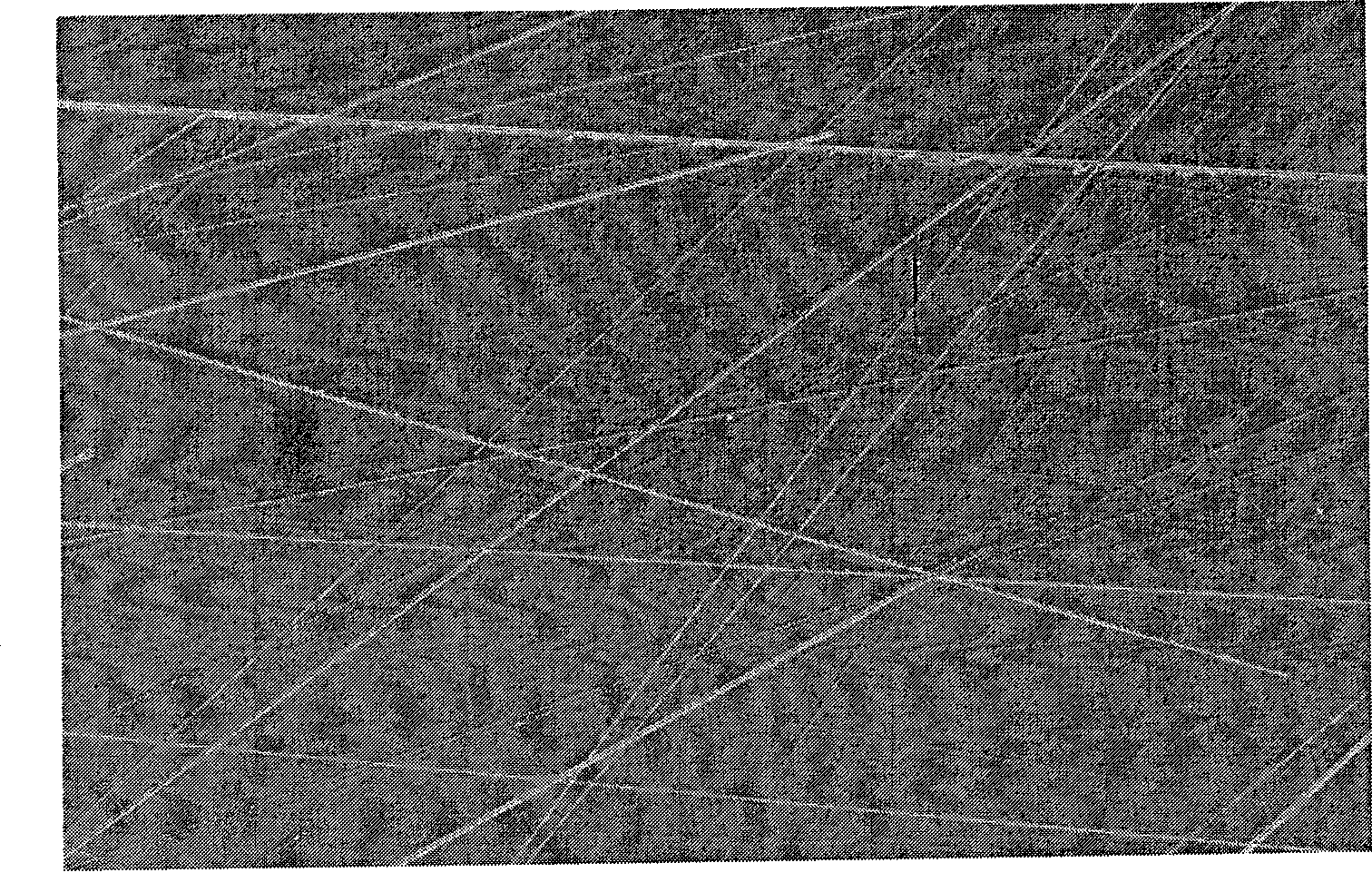
[0041] The surface morphology of the prepared s...
Embodiment 3
[0043] The present invention adopts the chemical mechanical polishing method to prepare the Si substrate. The specific polishing method and polishing result are the same as in Example 1, the difference is that during grinding and chemical mechanical polishing, the pressure on the control wafer is 500g / cm 2 , the suspending agent used is polyethylene glycol; when grinding, use alumina micropowder with a particle size of 50 μm, and the weight ratio of the micropowder, water and suspending agent in the grinding liquid is 1:200:100; during chemical mechanical polishing, use particle size It is 15μm boron carbide or alumina micropowder, the polishing disc is tin plate, the dispersant used is sodium silicate or sodium hexametaphosphate or ammonia water, the ratio of micropowder, water, dispersant and suspending agent in the polishing liquid is 1:1 :0.1:1. After chemical mechanical polishing, the annealing temperature of the wafer is 500° C., and the holding time is 10 hours.
[004...
PUM
| Property | Measurement | Unit |
|---|---|---|
| Granularity | aaaaa | aaaaa |
| Granularity | aaaaa | aaaaa |
| Granularity | aaaaa | aaaaa |
Abstract
Description
Claims
Application Information