P-zinc oxide/N- nickel oxide heterogeneous PN junction ultraviolet laser diode and method for production

An ultraviolet laser and pn junction technology, which is applied in the fields of nanomaterials and optoelectronic devices, can solve the problems of low mobility and poor stability of p-ZnO, and achieve the effects of improving luminescence performance, improving performance and simple preparation process.

Active Publication Date: 2009-08-12
常熟紫金知识产权服务有限公司
View PDF0 Cites 21 Cited by
  • Summary
  • Abstract
  • Description
  • Claims
  • Application Information

AI Technical Summary

Problems solved by technology

Reported (Sheng Chu, Mario Olmedo, Zheng Yang, Jieying Kong, and Jianlin Liu, Electrically pumped ultraviolet ZnO diode lasers on Si, APPLIED PHYSICSLETTERS 93, 181106_2008_) ZnO homojunction ultraviolet lasing diodes need to do multilayer quantum well structure , and the p-ZnO used has low mobility and poor stability

Method used


Image

  • P-zinc oxide/N- nickel oxide heterogeneous PN junction ultraviolet laser diode and method for production
  • P-zinc oxide/N- nickel oxide heterogeneous PN junction ultraviolet laser diode and method for production
  • P-zinc oxide/N- nickel oxide heterogeneous PN junction ultraviolet laser diode and method for production

Examples


preparation example Construction

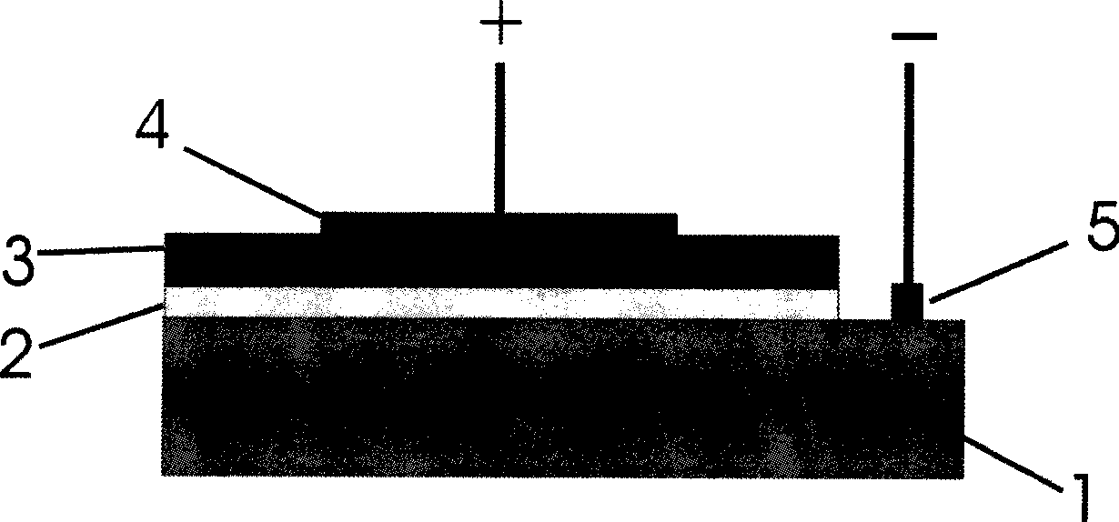
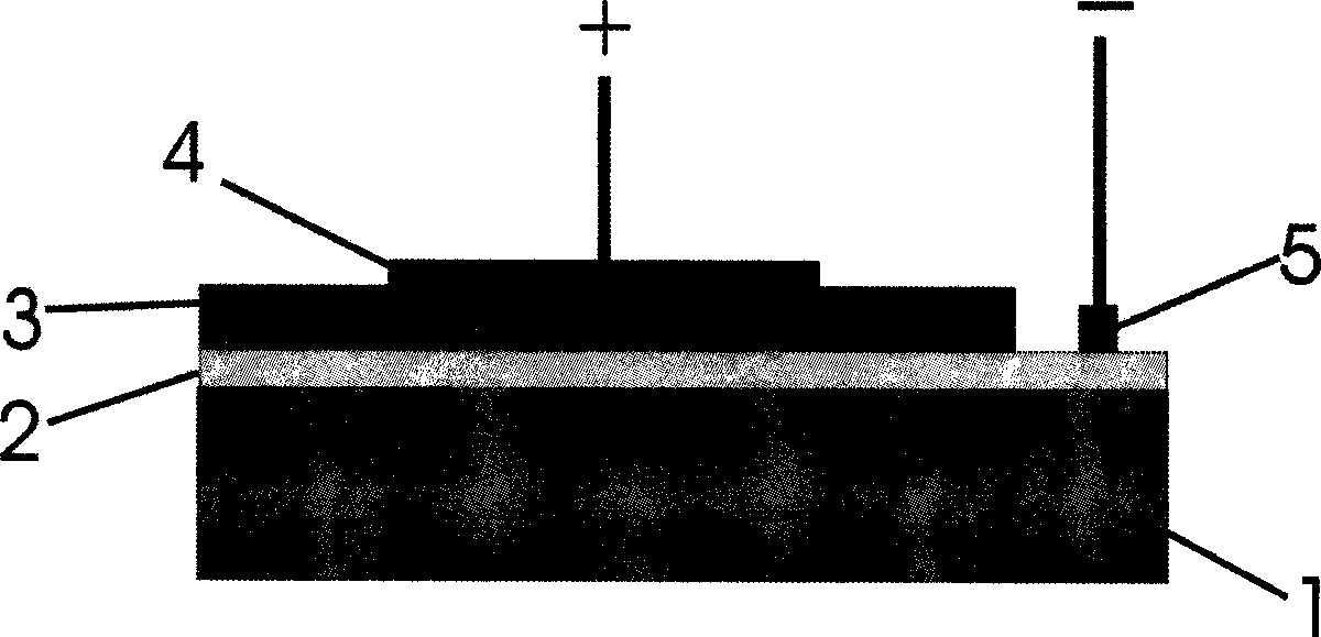
[0020] (3) Preparation of p-NiO: A Ni metal target with a diameter of 50 mm was used. According to the report of people such as I.Hotovy (I.Hotovy, J.Huran, J. et al., Deposition and properties of nickel oxide films produced by DC reactive magnetron sputtering, Vacuum, 1998, 51 (2): 157.), the NiO film prepared by magnetron reactive sputtering, when the O in the mixed atmosphere 2 When the ratio increases, the resistivity of the film will increase, while the light transmittance will decrease. In order to make the NiO film have high electrical conductivity and light transmittance at the same time, the relative oxygen partial pressure O 2 / (O 2 +Ar) = 50-70% of the optimal amount. The chamber background vacuum degree before sputtering is greater than 5×10 -4 Pa, the sputtering pressure is 0.5-1.5Pa, and the sputtering power is 100-250W. Before coating, pre-sputter for 10 min to remove impurities on the target surface. NiO film is plated on the substrate with ZnO thin film....

Embodiment 1

[0026] 1. Substrate cleaning: Use n-type GaN grown on sapphire as the substrate, cut it into a size of 25mm×30mm, ultrasonically clean it with acetone, alcohol, and deionized water for 3 minutes, and finally dry it with a nitrogen gun.

[0027] 2. Growth of n-type layer ZnO: Deposit ZnO thin film 2 on GaN1 by radio frequency magnetron sputtering. The target material is ZnO ceramic target, and the background vacuum is 1*10 -3 pa, deposition substrate temperature: 300°C; deposition pressure: 0.5Pa; relative oxygen partial pressure O 2 / (O 2 +Ar)=15%, power 150W; sputtering time: 15min.

[0028]3. Preparation of p-NiO: NiO film 3 was deposited on the ZnO nano film by reactive sputtering. The target material is made of high-purity metal Ni target, and the background vacuum is 4*10 -4 pa, deposition substrate temperature: 150°C; deposition pressure: 1.5Pa, relative oxygen partial pressure O 2 / (O 2 +Ar)=50%; power: 100W, sputtering time: 80min.

[0029] 4. Electrode preparat...

Embodiment 2

[0032] 1. Substrate cleaning: Use n-type GaN grown on sapphire as the substrate, cut it into a size of 25mm×30mm, ultrasonically clean it with acetone, alcohol, and deionized water for 3 minutes, and finally dry it with a nitrogen gun.

[0033] 2. Growth of n-type layer: deposit ZnO thin film 2 on GaN1 by radio frequency magnetron sputtering. The target material is ZnO ceramic target, and the background vacuum is 8*10 -4 pa, deposition substrate temperature: 100°C; deposition pressure: 5.0Pa; relative oxygen partial pressure O 2 / (O 2 +Ar)=40%, power 80W; sputtering time: 40min.

[0034] 3. Preparation of p-NiO: A NiO thin film 3 was deposited on a glass sheet with ZnO nanorods by reactive sputtering. The target material is high-purity metal Ni target, and the background vacuum is 5*10 -4 pa, deposition substrate temperature: 400°C; deposition pressure: 0.5Pa, relative oxygen partial pressure O 2 / (O 2 +Ar)=70%; power: 250W, sputtering time: 30min.

[0035] 4. Electrode...


PUM

PropertyMeasurementUnit
wavelengthaaaaaaaaaa
widthaaaaaaaaaa

Abstract

The invention discloses an n -zinc oxide/ p- nickel oxide heterogeneous pn junction ultraviolet laser diode and a preparation method thereof. The heterogeneous pn junction diode at least comprises a pn junction, a substrate and an ohm contacting electrode, wherein the pn junction is the heterogeneous pn junction by plating a p-type nickel oxide film on an n-type zinc oxide film; and the substrate is a sapphire plated with n-type GaN. The preparation method comprises the following steps: firstly preparing the n-type ZnO film layer on the substrate by the radio frequency magnetron sputtering technology; then sputtering a p-type NiO film layer on the n-type ZnO film layer to form the heterogeneity pn junction; finally manufacturing a pn junction electrode by a sputtering method or a thermal evaporation method; sputtering gold electrodes or platinum electrodes or nickel platinum electrodes or ITO electrodes on the NiO surface; plating indium electrodes or aluminum electrodes or gold electrodes on the GaN or the edge of ZnO; and making the electrodes form ohm contact after annealing alloying. The heterogeneous pn junction diode has the advantages of better electro-ultraviolet lasing luminescence characteristic, peak luminous wavelength of about 375 nm, simple preparation process and low cost.

Description

technical field [0001] The invention relates to an n-zinc oxide / p-nickel oxide heterogeneous pn junction ultraviolet laser diode and a preparation method thereof, belonging to the field of nanometer materials and optoelectronic devices. Background technique [0002] Zinc oxide (ZnO) is a new type II-VI direct bandgap wide bandgap semiconductor material. The band gap of ZnO is 3.37eV at room temperature, and the emission wavelength is equivalent to the wavelength of near-ultraviolet light (370nm), which is very suitable for making short-wavelength light-emitting and photosensitive devices. ZnO is similar to GaN in terms of lattice structure, unit cell parameters and forbidden band width, and has a higher melting point and greater exciton binding energy than GaN, and has lower photoluminescence and stimulated emission. Threshold value and good electromechanical coupling characteristics, thermal stability and chemical stability. Therefore, it has great potential in the applic...

Claims


Application Information

Patent Timeline
Patent Type & Authority Applications(China)
IPC IPC(8): H01S5/32H01S5/327H01L21/203C23C14/35C23C14/26C23C14/08H01L21/28
Inventor 方国家黄晖辉莫小明龙浩
Owner 常熟紫金知识产权服务有限公司
Why Eureka
Try Eureka