P-type CuxSy semiconductor nanocrystalline, preparation method and application thereof

A nanocrystal and semiconductor technology, applied in semiconductor/solid-state device manufacturing, semiconductor device, nanotechnology, etc., can solve the problem of single crystal phase, and achieve the effect of single crystal phase, good electrical conductivity, and high carrier mobility.

Inactive Publication Date: 2012-11-14
BEIJING INSTITUTE OF TECHNOLOGYGY +1
View PDF3 Cites 17 Cited by
  • Summary
  • Abstract
  • Description
  • Claims
  • Application Information

AI Technical Summary

Problems solved by technology

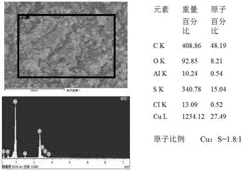
[0004] Aiming at the inability to obtain Cu with a single crystal phase, good dispersion, and controllable size and shape at this stage x S y The defect of semiconductor nanocrystal, the present invention provides a kind of p-type Cu x S y Semiconductor nanocrystals (x / y=1.8)

Method used


Image

  • P-type CuxSy semiconductor nanocrystalline, preparation method and application thereof
  • P-type CuxSy semiconductor nanocrystalline, preparation method and application thereof
  • P-type CuxSy semiconductor nanocrystalline, preparation method and application thereof

Examples


Embodiment 1

[0041] A p-type Cu of the present invention x S y A method for preparing semiconductor nanocrystals, the method steps are as follows:

[0042] Step 1: Prepare the copper source

[0043] Add 0.398g cuprous chloride, 2ml oleic acid, 1.5ml oleylamine and 1.5ml octadecene into a 25ml three-necked round bottom flask to obtain mixed solution 1. Vacuum the mixed solution 1 for 30 minutes, and then pass it into nitrogen protection , Under stirring conditions, heat the mixed solution 1 to 130°C and keep it for 30 minutes to form a uniform transparent dark green solution to obtain a copper source;

[0044] Step 2: Preparation of sulfur source

[0045] Add 0.064g of sulfur powder to a 50ml three-necked round-bottom flask, and then add 10ml of octadecene to obtain a turbid mixed solution 2. Vacuum the mixed solution 2 for 30 minutes, then pass it into nitrogen protection, and mix the mixed solution 2 under stirring conditions Heat to 180°C and keep for 10 minutes to form a uniform and transparen...

Embodiment 2

[0051] A p-type Cu of the present invention x S y A method for preparing semiconductor nanocrystals, the method steps are as follows:

[0052] Step 1: Prepare the copper source

[0053] Add 0.398g of cuprous chloride, 4ml of oleic acid, and 1.5ml of oleylamine into a 25ml three-necked round bottom flask to obtain mixed solution 1. Vacuum the mixed solution 1 for 30 minutes, and then pass it into nitrogen protection. The mixed solution 1 is heated to 90°C and kept for 30 minutes to form a uniform transparent dark green solution to obtain a copper source;

[0054] Step 2: Preparation of sulfur source

[0055] Add 0.032g of sulfur powder to a 50ml three-necked round-bottom flask, and then add 10ml of octadecene to obtain a turbid mixed solution 2. Vacuum the mixed solution 2 for 30 minutes, and then pass it into nitrogen protection, and mix the mixed solution 2 with stirring. Heat to 200°C and keep it for 10 minutes to form a uniform and transparent yellow solution to obtain a sulfur so...

Embodiment 3

[0061] A p-type Cu of the present invention x S y A method for preparing semiconductor nanocrystals, the method steps are as follows:

[0062] Step 1: Prepare the copper source

[0063] Add 13.500g of copper chloride, 50ml of oleic acid, and 40ml of oleylamine into a 250ml three-necked round bottom flask to obtain mixed solution 1. Vacuum the mixed solution 1 for 30 minutes, then pass it into nitrogen protection, and mix the solution under stirring 1 Heat to 150°C and keep for 30 minutes to form a uniform transparent dark green solution to obtain a copper source;

[0064] Step 2: Preparation of sulfur source

[0065] Add 1.6g of sulfur powder to a 250ml three-necked round bottom flask, and then add 100ml of octadecene to obtain a turbid mixed solution 2. The mixed solution 2 is evacuated for 30 minutes, and then nitrogen is protected. Under stirring, the mixed solution 2 Heat to 300°C and keep for 10 minutes to form a uniform and transparent yellow solution to obtain a sulfur source;...


PUM

PropertyMeasurementUnit
particle diameteraaaaaaaaaa
thicknessaaaaaaaaaa

Abstract

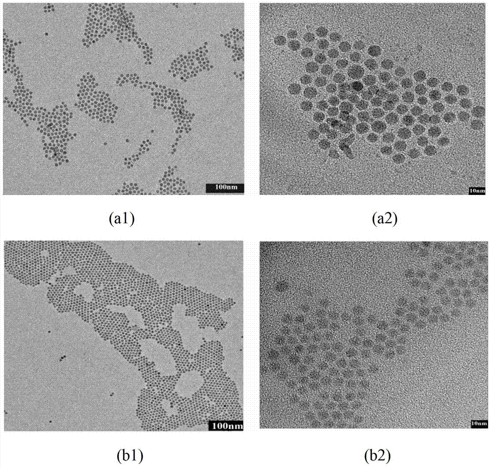
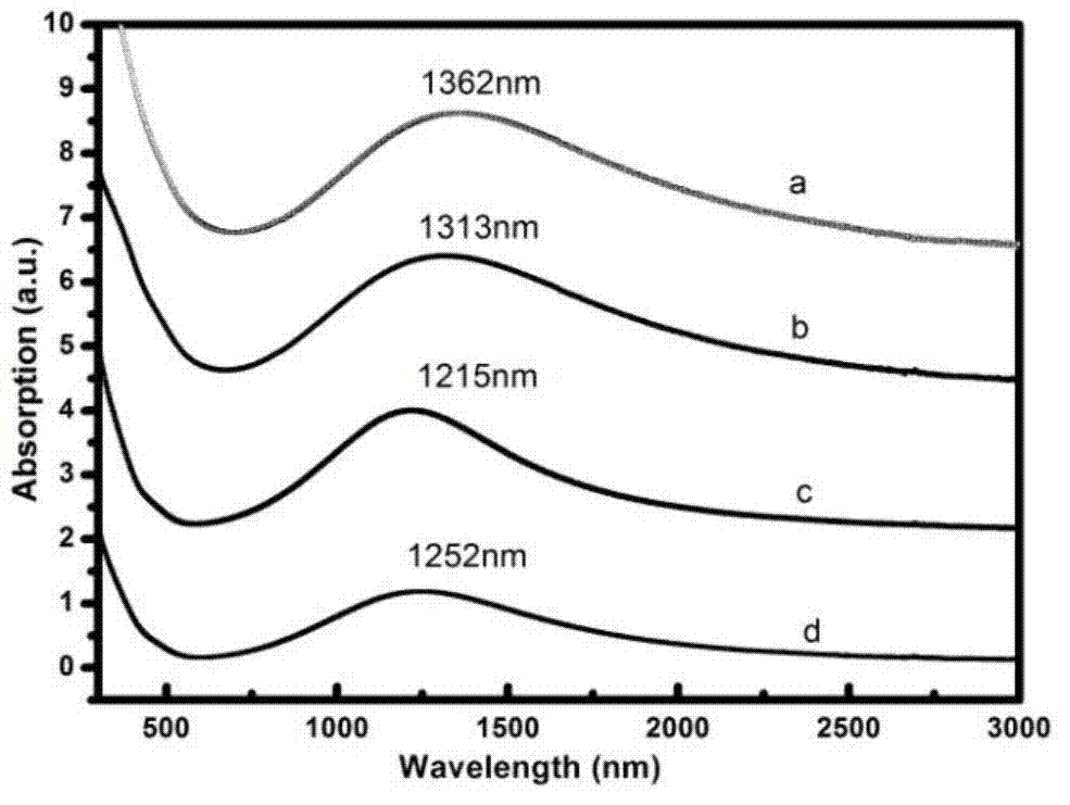
The invention discloses a p-type CuxSy semiconductor nanocrystalline, a preparation method and an application thereof and belongs to the fields of nanometer material preparation and applications. X/y of the nanocrystalline CuxSy is 1.8, the nanocrystalline is spherical, and the particle size of the nanocrystalline is 6-12nm. The preparation method includes preparing a copper source, preparing a sulfur source, injecting the copper source to the sulfur source, subjecting the solution to heating reaction to obtain a colloidal solution and subjecting the colloidal solution to washing and centrifugal sedimentation to obtain the nanocrystalline. The nanocrystalline is single in crystalline phase, good in dispersibility, controllable in size and morphology, good in electrical conductivity, high in carrier mobility and good in high temperature resistance and stability, the nanocrystalline is high in absorption ability in the whole near infrared area, and the absorption peak is 1100-1500nm. The preparation method is high in productivity and applicable to large-scale production. When the nanocrystalline is applicable to hole transport layers of thin-film solar cells, transport abilities of the hole transport layers can be obviously improved.

Description

Technical field [0001] The invention relates to a p-type Cu x S y Semiconductor nanocrystals, preparation methods and applications thereof belong to the field of nanomaterial preparation and application. Background technique [0002] Copper-containing chalcogenide semiconductor nanocrystals, such as Cu x S y , Cu x Se y And Cu x Te y , Has excellent photoelectric conversion, photothermal conversion and thermoelectric conversion performance, and has important applications in the fields of solar cells, photodetectors, lithium ion battery electrode materials, photocatalytic degradation materials, and near-infrared photothermal therapy. In recent years, the preparation methods of such semiconductor nanocrystals include sonochemical synthesis, electrochemical synthesis and thermal cracking synthesis. For example, LinSong Li first synthesizes copper stearate, then dissolves the copper stearate in octadecene, and uses dodecyl mercaptan (DDT) as the sulfur source to synthesize Cu with a ...

Claims


Application Information

Patent Timeline
Patent Type & Authority Applications(China)
IPC IPC(8): C01G3/12B82Y40/00H01L51/46
CPCY02E10/549Y02P70/50
Inventor 钟海政张腾刘立格邹炳锁谢海燕
Owner BEIJING INSTITUTE OF TECHNOLOGYGY
Why Eureka
Try Eureka