BeMgZnO-based MSM solar blind detector and preparation method thereof

An ultraviolet detector, 3.37ev technology, applied in the field of ultraviolet detectors, can solve the problems of bulky volume, reduced quantum efficiency, limited energy band adjustment, etc., and achieves the effects of good light response, simple preparation process, and easy portability

Inactive Publication Date: 2013-04-03
SUN YAT SEN UNIV
View PDF2 Cites 10 Cited by
  • Summary
  • Abstract
  • Description
  • Claims
  • Application Information

AI Technical Summary

Problems solved by technology

[0004] (1) The photomultiplier tube needs to work under high voltage, so it needs to be equipped with a high voltage source, which is bulky and easily damaged
[0005] (2) Silicon UV detector has three obvious disadvantages: 1. It has a strong absorption of visible light, so it needs to be accompanied by a complex filter system, which increases the cost; 2. It has a strong absorption of ultraviolet light, causing ultraviolet light The penetration depth is very shallow,

Method used


Image

  • BeMgZnO-based MSM solar blind detector and preparation method thereof
  • BeMgZnO-based MSM solar blind detector and preparation method thereof
  • BeMgZnO-based MSM solar blind detector and preparation method thereof

Examples


Embodiment 1

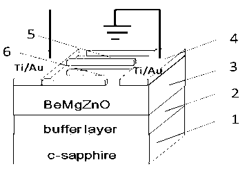
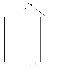
[0032] Such as figure 1 , 2 Shown in and 3, a kind of BeMgZnO-based MSM structure ultraviolet detector comprises a substrate 1, a buffer layer 2 is deposited on the substrate 1, a thin film layer 3 is grown on the buffer layer 2; a metal contact is made on the thin film layer 3 The pattern of the interdigitated electrodes 4, the gap between the interdigitated electrodes 4 is the photosensitive area 6.

[0033] The film layer 3 is a BeMgZnO quaternary alloy film layer, and the thickness of the BeMgZnO quaternary alloy film layer is 200nm~1um; the BeMgZnO quaternary alloy film layer adjusts the band gap by adjusting the atomic ratio of the three elements of beryllium, magnesium and zinc, The forbidden band width is 3.37eV~6.2eV.

[0034] In this embodiment, when the substrate is sapphire polished on both sides, the orientation of the sapphire polished on both sides is c-orientation. The interdigitated electrodes are made of titanium (Ti) and gold (Au).

[0035] The preparati...

Embodiment 2

[0041] This embodiment is the same as Embodiment 1 except for the following features: In this embodiment, in step 4), the interdigitated electrodes are selected from titanium (Ti), aluminum (Al), nickel (Ni), gold (Au) , platinum (Pt), silver (Ag), iridium (Ir), molybdenum (Mo), tantalum (Ta), niobium (Nb), cobalt (Co), zirconium (Zr) and tungsten (W) and other metals. The required metal can be selected according to the needs. For example, platinum (Pt) has a higher work function, and the electrode can form a Schottky contact; while titanium (Ti), aluminum (Al), and gold (Au) can form an ohmic contact.

[0042]

Embodiment 3

[0044] This embodiment is the same as Embodiment 1 except for the following features: In this embodiment, in step 3), a thin film layer is grown on the buffer layer by chemical vapor deposition (MOCVD).


PUM

PropertyMeasurementUnit
Thicknessaaaaaaaaaa
Thicknessaaaaaaaaaa
Deposition thicknessaaaaaaaaaa

Abstract

The invention discloses a BeMgZnO-based MSM structure ultraviolet detector and a preparation method thereof. The ultraviolet detector comprises a substrate, and is characterized in that a buffer layer is deposited on the substrate, and a film layer grows on the buffer layer; interdigital electrode patterns as metallic contacts are formed on the film layer, and a clearance part between the interdigital electrodes is a photosensitive area; the film layer is a BeMgZnO quaternary alloy film layer, and the thickness of the BeMgZnO quaternary alloy film layer is in the range of tens of nanometers to several microns; and the forbidden bandwidth of the BeMgZnO quaternary alloy film layer is regulated by regulating the atom proportioning of the three elements Be, Mg and Zn, and the forbidden bandwidth is 3.37 eV-6.2 eV. According to the invention, by adopting the BeMgZnO quaternary alloy film layer as the absorption layer, the ultraviolet detector responding in the solar blind range of 200nm-375 nm is obtained, thus covering the whole solar blind region.

Description

technical field [0001] The invention relates to the technical field of ultraviolet detectors, in particular to a BeMgZnO-based MSM solar-blind detector and a preparation method thereof. Background technique [0002] Ultraviolet detection is another important detection technology developed after infrared detection and laser detection, which is widely used in military affairs and daily life. For the military, since jets, rockets and missiles radiate a large amount of ultraviolet rays during launch and flight, the developed ultraviolet detection technology will help improve our space defense and ensure our homeland security. In civil use, ultraviolet detection is also widely used, such as the monitoring of combustible gas in mines and automobile exhaust, environmental pollution monitoring, DNA testing and submarine oil spill monitoring, etc. [0003] At present, commercial ultraviolet detectors mainly include silicon ultraviolet detectors, photomultiplier tubes and GaN wide ba...

Claims


Application Information

Patent Timeline
IPC IPC(8): H01L31/103H01L31/0296H01L31/18
CPCY02P70/50
Inventor 汤子康祝渊苏龙兴张权林陈明明陈安琪桂许春项荣吴天准
Owner SUN YAT SEN UNIV
Why Eureka
Try Eureka