

High temperature oxidation resistant film sensor and production method thereof
A thin film sensor, high temperature oxidation resistance technology, applied in metal material coating process, superimposed layer plating, coating and other directions, can solve the problem of ITO thin film resistivity increase, affecting performance stability, reliability and measurement accuracy, The problem of carrier concentration decline, etc., achieves excellent anti-oxidation and insulating properties, good blocking of sodium ions, and high chemical stability.
- Summary
- Abstract
- Description
- Claims
- Application Information
AI Technical Summary
Problems solved by technology
Method used
Image

Examples
Embodiment 1
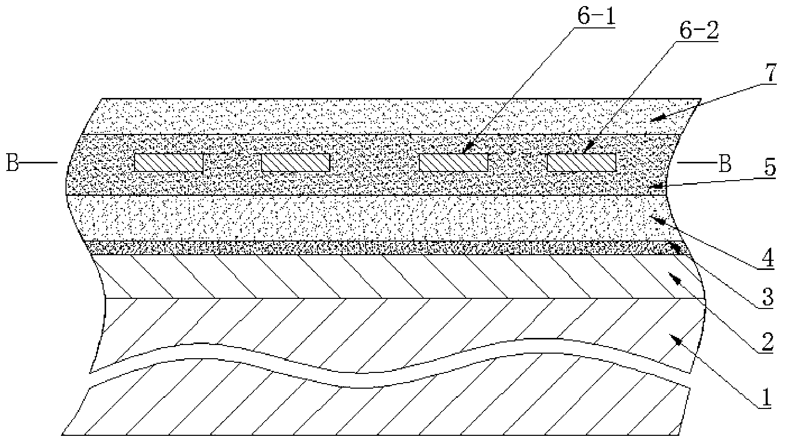
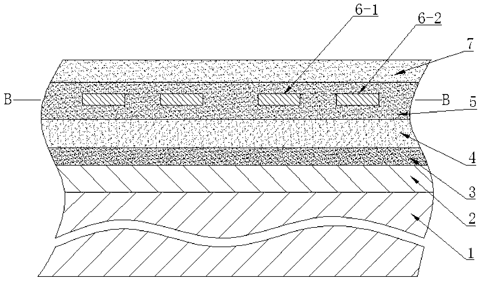
[0033] Example 1: Take a nickel (Ni)-based alloy plate as the alloy substrate 1 to be tested, prepare an ITO thermocouple film sensor on it, and select silicon nitride as the protective layer material as an example:
[0034] 1) Surface treatment of the alloy substrate: a nickel (Ni)-based alloy plate (length×width×thickness) 30×95×5mm is used as the alloy substrate 1 to be tested, and the surface of the alloy substrate to be tested is firstly and then treated with acetone and ethanol. Cleaning, drying under nitrogen atmosphere after cleaning;
[0035] 2) Deposit a NiCrAlY alloy transition layer on the alloy substrate: put the cleaned Ni-based alloy substrate 1 in a vacuum of 6.0×10 -4 In a vacuum environment of Pa (i.e. background vacuum), NiCrAlY alloy is used as the target material, and argon gas with a purity of 99.999% (volume percentage) is input as the sputtering medium. ) under the condition of 0.6Pa, the NiCrAlY alloy was deposited on the Ni-based alloy substrate 1 by...
Embodiment 2
[0042] Example 2: A nickel (Ni)-based alloy plate is used as the alloy substrate to be tested, and a K-type NiCr-NiSi thermocouple thin film sensor is prepared on it:
[0043] This embodiment specifically implements steps 1), 2), 3), 4), 5), and 6) and the process conditions and parameters of A, B, C, D, E, and F in the specific implementation of the invention patent application publication specification CN102212823A correspond to the same;
[0044] 7) Set the thin film sensor functional layer and its Si 3 N 4 Isolation layer: first place the composite substrate prepared in step 6) on the back and the vacuum degree is 6.0×10 -4 In the CVD processing device of Pa, SiH is used 4 / NH 3 (flow ratio for SiH 4 : NH 3 =1:9) As the air source, the vacuum degree of the back and bottom is 6.0×10 -4 Pa, the working pressure is 60Pa, the deposition temperature is 270°C, the RF power is 20W, and the Si 3 N 4 Deposited on a composite substrate to obtain Si with a thickness of 1 μm ...
Embodiment 3
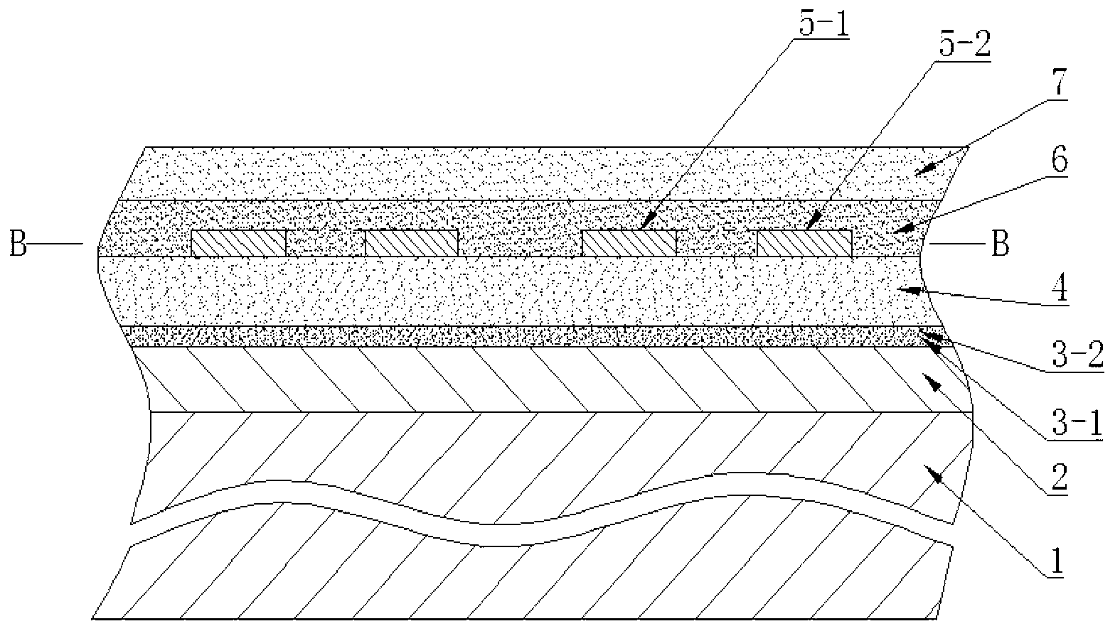
[0046] Example 3: A nickel (Ni)-based alloy plate is used as the alloy substrate to be tested, and a K-type NiCr-NiSi thermocouple film sensor is prepared on it:
[0047] The specific implementation steps 1), 2), 3), 4) and 5) of this embodiment and the process conditions and process conditions of 1), 2), 3), 4) and 5) disclosed in the specific implementation methods disclosed in the patent application publication CN101894904A The parameters correspond to the same;
[0048] 6) Set the thin film sensor functional layer and its Si 3 N 4 Isolation layer: First, the vacuum on the backside is 6.0×10 -4 Pa, with argon gas as the reaction medium, Ni90Cr10 and Ni97Si3 as the target materials, at room temperature, and under the conditions of 100W power and 0.4Pa working pressure, the surface of the AlN ceramic insulating layer 4 is sequentially deposited by conventional magnetron sputtering method Two NiCr-NiSi thermocouples with a thickness of 1 μm are used as (thin film) sensor fu...
PUM
| Property | Measurement | Unit |
|---|---|---|
| Thickness | aaaaa | aaaaa |
Abstract
Description
Claims
Application Information