Semiconductor device and manufacturing method thereof

A manufacturing method and semiconductor technology, applied in the field of microelectronics, can solve the problems that ordinary lithography machines cannot meet the process requirements and increase the difficulty of lithography process, and achieve the effects of improving electric field distribution, reducing electrode size, and increasing breakdown voltage

Active Publication Date: 2014-03-12
ENKRIS SEMICON
View PDF4 Cites 13 Cited by
  • Summary
  • Abstract
  • Description
  • Claims
  • Application Information

AI Technical Summary

Problems solved by technology

However, such a fine size greatly increases the difficulty of the lithography process. Ordinary lithography machines cannot meet the process requirements, and electron beam lithography machines are needed to achieve smaller line widths.

Method used


Image

  • Semiconductor device and manufacturing method thereof
  • Semiconductor device and manufacturing method thereof
  • Semiconductor device and manufacturing method thereof

Examples


Embodiment 1

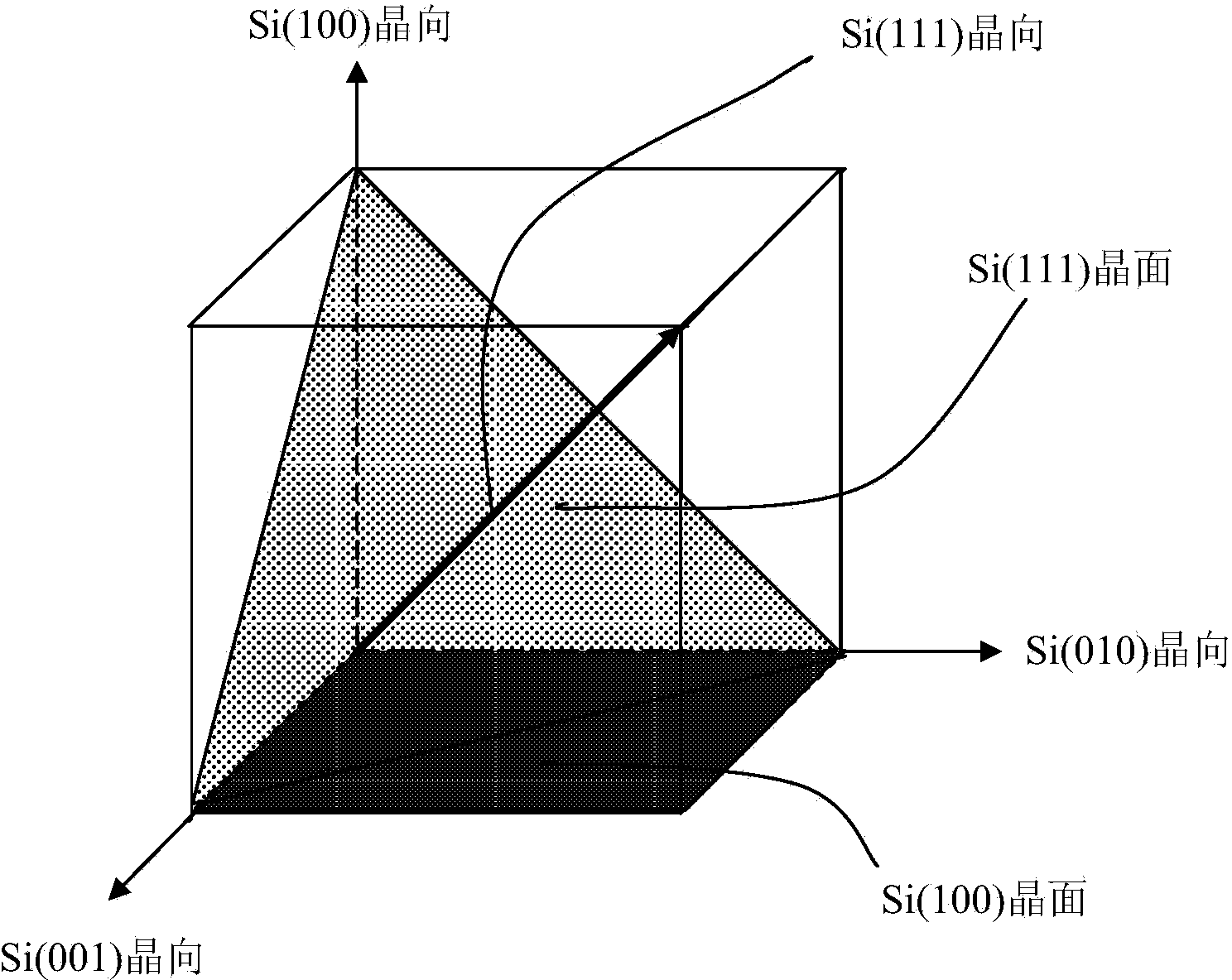
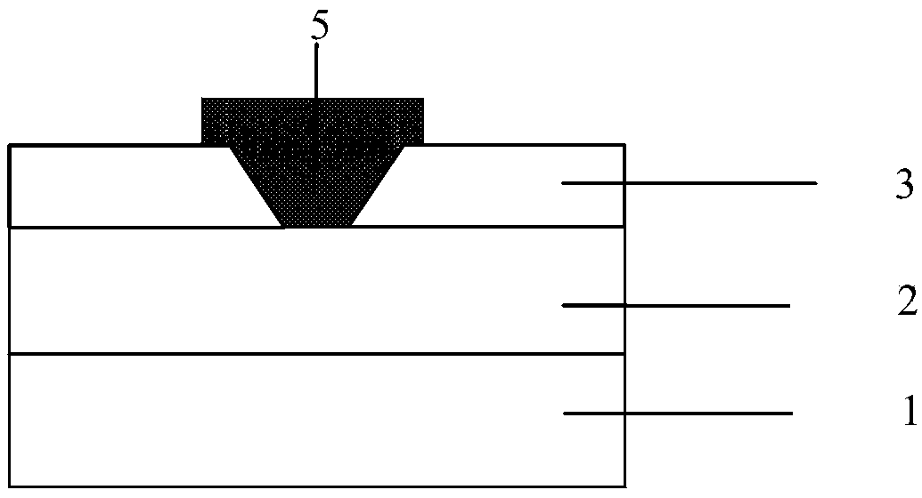
[0069] As shown in Figure 2 (a), the semiconductor device includes: a substrate 1; a gallium nitride semiconductor layer 2 on the substrate 1; an additional layer 3 of silicon semiconductor on the semiconductor layer 2; A groove formed by etching; an electrode 4 formed at the groove. In this embodiment, the substrate 1 may be silicon, silicon carbide, germanium, silicon-on-sapphire or sapphire. In this embodiment, the semiconductor device can be a Schottky diode, or a metal insulator field effect transistor (MISFET), including a metal oxide field effect transistor (MOSFET), or a metal semiconductor field effect transistor (MESFET), high Electron Mobility Transistor (HEMT) or Heterojunction Field Effect Transistor (HFET). In this embodiment, the semiconductor layer may be any one or a combination of silicon, germanium, gallium arsenide, gallium nitride, aluminum nitride, aluminum gallium nitride, and aluminum gallium indium nitrogen.

[0070] Such as Figure 2(b) , 2(c) , 2...

Embodiment 2

[0073] The semiconductor device includes: a substrate 1 , a semiconductor layer 2 , a passivation layer 3 , an additional layer 4 and an electrode 5 . This implementation mode is different from Example 1 in that a passivation dielectric layer 3 is added between the semiconductor layer 2 and the additional layer 4 . The passivation dielectric layer 3 may comprise one or a combination of silicon nitride, silicon germanium nitrogen, silicon aluminum gallium nitrogen, silicon aluminum oxide, aluminum magnesium oxygen nitrogen, silicon aluminum nitrogen and silicon dioxide.

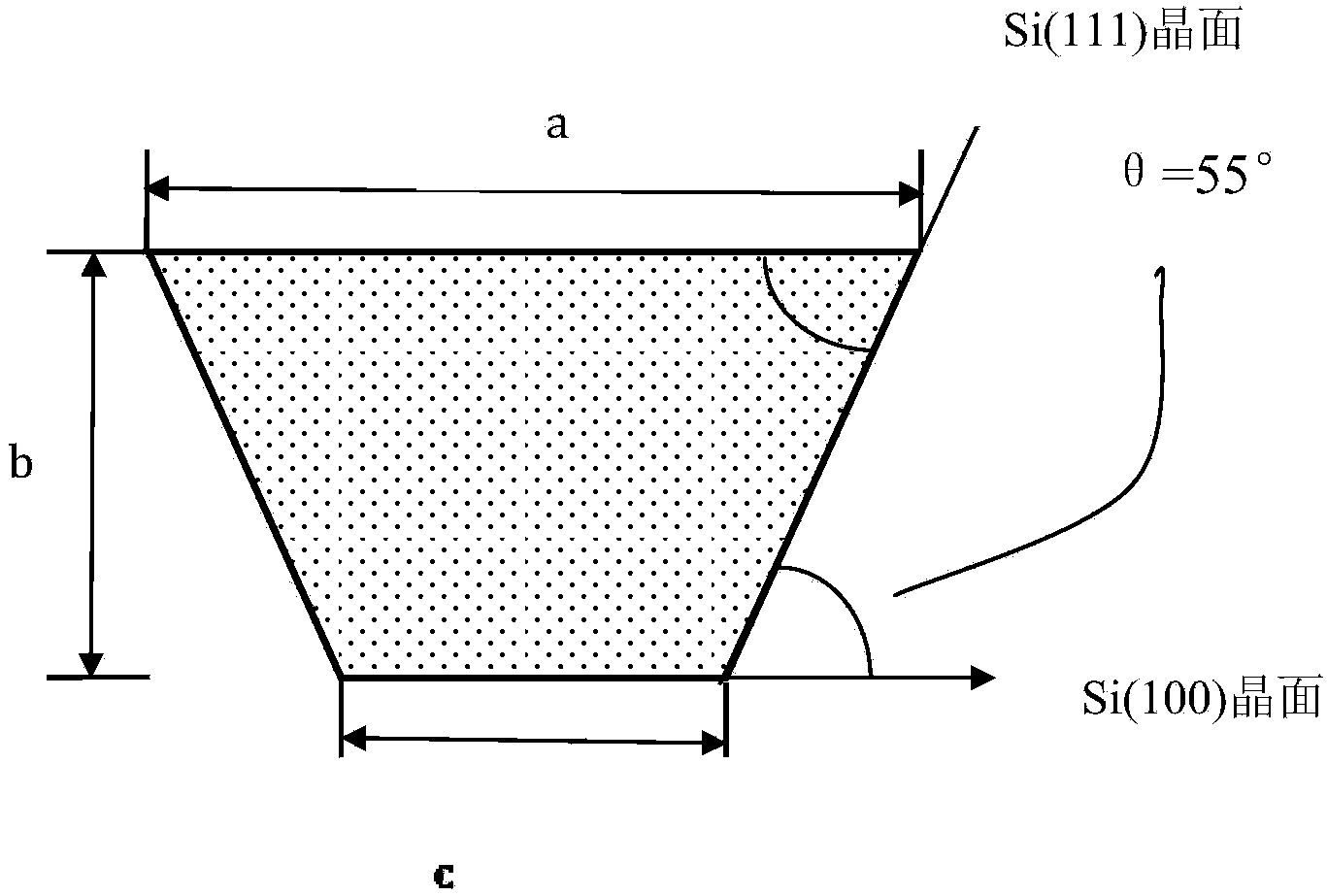
[0074] As shown in Figure 3(a), Figure 3(b), Figure 3(c) and Figure 3(d), after forming an inverted trapezoidal electrode groove by etching the additional layer 4, that is, the silicon (100) thin film semiconductor layer, The size of the electrode groove can be greatly reduced. Then, by etching the silicon nitride passivation layer 3 below the trapezoidal groove, the groove of the silicon nitride layer 3 form...

Embodiment 3

[0076] The semiconductor device includes: a substrate 1 , a semiconductor layer 2 , a passivation layer 3 , an additional layer 4 and an electrode 5 . Compared with Example 2, the difference of this embodiment is that, as Figure 4 As shown, a passivation dielectric layer 3 is added between the active semiconductor layer 2 and the silicon additional layer 4, and after the electrode metal with improved structure is formed in the electrode groove, the silicon additional layer 4 is oxidized to form a silicon dioxide layer 4, and The silicon additional layer 4 is not removed. In this way, a silicon dioxide layer 4 can be added on the passivation layer 3 to function as a dielectric layer and a protective layer. The passivation dielectric layer 3 may comprise one or a combination of silicon nitride, silicon germanium nitrogen, silicon aluminum gallium nitrogen, silicon aluminum oxide, aluminum magnesium oxygen nitrogen, silicon aluminum nitrogen and silicon dioxide. Other structur...


PUM

PropertyMeasurementUnit
widthaaaaaaaaaa
thicknessaaaaaaaaaa

Abstract

The invention discloses a manufacturing method of a semiconductor device. The method comprises the steps of sequentially forming a semiconductor layer, a silicon additional layer and a photolithographic mask layer on a substrate; etching the partial area of the silicon additional layer, thus forming an oblique section along a crystal plane of silicon (111) and forming a trapezoid groove together with a crystal plane of silicon (100), which is not etched, till the semiconductor layer is exposed; and finally, depositing metal in the groove, thus forming an electrode. The semiconductor device manufactured by the method disclosed by the invention has the advantages that the structure and the shape of the electrode are controlled and optimized by virtue of the characteristic of anisotropism of the silicon additional layer in the etching process and the electric field distribution of the semiconductor layer can be improved, so that the breakdown voltage of the device is increased; in the meantime, the electrode size of the device can be effectively reduced, and the frequency characteristic and the like of the device can be further improved.

Description

technical field [0001] The invention belongs to the technical field of microelectronics, and in particular relates to a method for manufacturing a semiconductor device and a semiconductor device manufactured by the method. Background technique [0002] In the manufacturing process of semiconductor devices including triodes and diodes, the shape and structure of the gate of the triode or the anode of the diode often play a very critical role in many important characteristics of the device. In a field-effect transistor, the shape and structure of the gate have an important influence on the distribution of charges in the semiconductor layer, and thus have an important impact on the magnitude of the electric field strength and the distribution of the potential. For example, in GaN high electron mobility transistor (HEMT), when the source-drain voltage is high (such as more than 100V), there is a peak of electric field intensity at the edge of the gate close to the drain, which i...

Claims


Application Information

Patent Timeline
Patent Type & Authority Applications(China)
IPC IPC(8): H01L21/28H01L29/423
CPCH01L21/28H01L29/423H01L21/28114H01L29/2003H01L29/42316H01L29/42376H01L29/66212H01L29/872
Inventor 程凯
Owner ENKRIS SEMICON
Why Eureka
Try Eureka