
A kind of preparation method of bulge sample of layered electromagnetic thin film functional material

A thin-film material and thin-film technology, which is applied in the field of preparation of layered electromagnetic thin film bulging samples, can solve the problems of small thickness of brittle pure films, difficult to apply directly, and difficult to directly apply bulging mechanical experimental test, etc. Simple, low-corrosion-condition effect

Active Publication Date: 2016-01-27
湖南新生代新材料科技有限公司
View PDF5 Cites 0 Cited by
  • Summary
  • Abstract
  • Description
  • Claims
  • Application Information

AI Technical Summary

Problems solved by technology

This thin film sample is mainly used in electrical performance testing. Since the thickness of this brittle pure thin film is very small, it is difficult to directly apply it to the bulging mechanical experiment test.
[0006] In short, it is difficult to directly apply the existing bulge sample preparation methods to layered electromagnetic thin film materials. Therefore, it is necessary to comprehensively consider the advantages of the size of the layered electromagnetic thin film material, the gel method and the advantages of the bulge test to improve the traditional bulge sample. The preparation method is to prepare an electromagnetic film bulge sample with a self-supporting window, and provide a reliable bulge sample for testing and analyzing its force-electromagnetic-thermal coupling performance in the multi-field environment of force, electricity, magnetism, and heat in the future.

Method used


Image

  • A kind of preparation method of bulge sample of layered electromagnetic thin film functional material
  • A kind of preparation method of bulge sample of layered electromagnetic thin film functional material
  • A kind of preparation method of bulge sample of layered electromagnetic thin film functional material

Examples


Embodiment 1

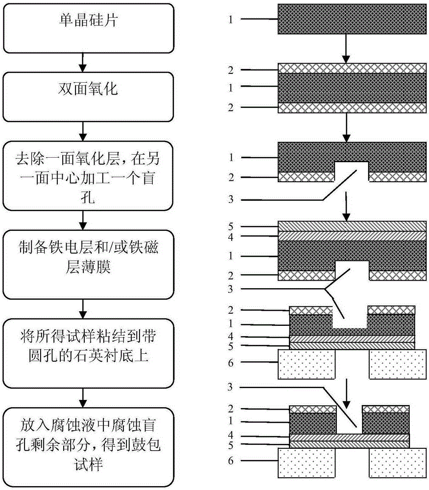
[0040] (1) Cut the 4-inch monocrystalline silicon wafer polished on one side into small square pieces, and then carry out high-temperature wet oxidation for 5 hours, and the oxidation temperature is 800°C. A layer of dense silicon dioxide 2 is formed on the upper and lower surfaces of the single crystal silicon wafer 1; the silicon dioxide 2 on a certain surface of the single crystal silicon wafer 1 is removed by grinding with metallographic sandpaper, and then cleaned with 40% hydrofluoric acid, Polished with 0.5 μm diamond micropowder. The silicon dioxide 2 on the other surface of the monocrystalline silicon wafer 1 remains.

[0041] (2) Use a micro-drilling machine with a diamond drill bit to gently and repeatedly grind and drill the center of the surface of the remaining silicon dioxide layer 2 to form a blind hole 3 with a diameter of 2 mm and a depth of 100 μm to 200 μm. The diameter and depth of the blind holes 3 can be changed as required, and can also be designed as...

Embodiment 2

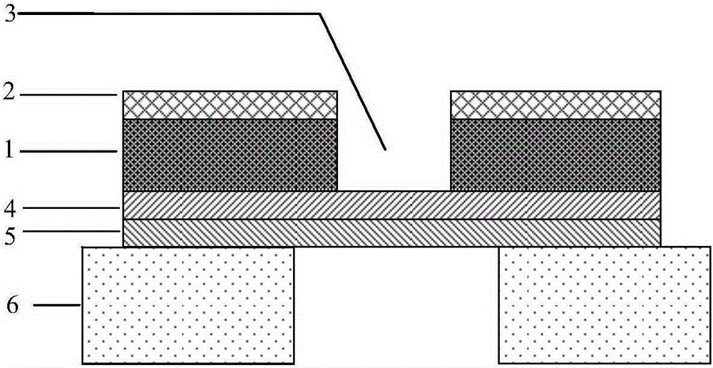
[0047] In this embodiment, the preparation method of the layered electromagnetic thin film bulge sample is basically the same as that in Example 1, except that in step (3) the sol-gel method is used in step (2) to obtain the single Bismuth sodium titanate ferroelectric thin film was prepared on the polished side of the crystalline silicon wafer. The number of homogenization times was 8, the heat treatment temperature was 420°C, and the annealing temperature was 700°C. The final film thickness obtained is 360nm, and the morphology of the obtained bismuth sodium titanate ferroelectric film is as follows: Figure 4 Shown, this is that steps (1), (2), (4), (5) and (6) in the embodiment are the same as in Example 1, and are prepared as image 3 Shown is a bulged specimen of layered electromagnetic material.

Embodiment 3

[0049] In the present embodiment, the preparation method of the layered electromagnetic thin film bulging sample is basically the same as that in Example 1, except that in step (4), heat-resistant and corrosion-resistant epoxy resin is used to seal the sample in step (4). ) to prepare the resulting sample; select 25% potassium hydroxide solution in step (5) and step (6), and the corrosion temperature is 40°C. All the other steps (1), (2), (3) and (4) are identical with embodiment 1, prepare as image 3 Shown is a bulged specimen of layered electromagnetic material.


PUM

PropertyMeasurementUnit
thicknessaaaaaaaaaa
thicknessaaaaaaaaaa
corrosion rateaaaaaaaaaa

Abstract

The invention discloses a method for preparing a bulging sample of layered electromagnetic film material. This method first uses wet oxidation and mechanical processing to process single crystal silicon wafers to obtain a single crystal silicon surface on one side and a silicon dioxide surface with specific blind holes on the other side. Then the electromagnetic thin film material is deposited on the single crystal silicon surface, and high-temperature annealing is completed. Then use organic silica gel to bond the side where the film material is deposited to a quartz substrate with a circular hole, and then seal the sample surface, exposing only the blind hole area. It is then put into a potassium hydroxide solution for etching, causing a chemical reaction to occur in the remaining substrate at the bottom of the blind hole area. The length of the etching time is determined based on the pre-calibrated etching rate until the single crystal silicon in this area is etched away and the film deposited on the other side of the sample is completely exposed. Then it is cleaned, dried and the organic silica gel is removed, and finally a bulging sample of the layered electromagnetic film material with an independent support window is obtained.

Description

technical field [0001] The invention relates to the technical field of layered electromagnetic thin film materials, in particular to a method for preparing a layered electromagnetic thin film bulge sample with a self-supporting window on a single crystal silicon substrate. Background technique [0002] Layered electromagnetic thin film functional materials are functional / smart materials with special magnetoelectric coupling response characteristics. Due to the heterogeneity, force-electromagnetic fully coupled physical-mechanical behavior, multi-scale interface coupling and many other superior properties, this kind of material has been widely used in aerospace, micro-electro-mechanical systems, optoelectronics, information storage systems, and smart sensor systems. And other fields, played an important role and significant economic benefits. In practical applications, such materials usually serve in thermal, force, electricity, and magnetic field coupling environments, and ...

Claims


Application Information

Patent Timeline
Patent Type & Authority Patents(China)
IPC IPC(8): H01L43/12H10N50/01
Inventor 毛卫国丁佳戴翠英肖敏周望谢敏方岱宁
Owner 湖南新生代新材料科技有限公司
Learn More