A Low Damage InGaAs Detector p + n-junction preparation method

An indium gallium arsenide and detector technology is applied in the field of preparation of infrared detectors, which can solve the problems of reducing surface state density, reducing recombination centers, and large junction damage, achieving a good process foundation, suppressing dark current, and suppressing the generation of Effect

Active Publication Date: 2017-03-22
无锡中科德芯感知科技有限公司
View PDF3 Cites 0 Cited by
  • Summary
  • Abstract
  • Description
  • Claims
  • Application Information

AI Technical Summary

Problems solved by technology

[0005] Based on the problems existing in the preparation process of the above-mentioned detector chip, the present invention proposes a low-damage InGaAs detector p + The n-junction preparation method can not only solve the problems of low activation of element ions, large junction damage and large electrode series resistance, but also increases the process of removing surface damage by wet etching, which removes the ion-enriched layer and reduces recombination. center, reducing the surface state density and enhancing the passivation effect of the subsequent passivation film

Method used


Image

  • A Low Damage InGaAs Detector p  <sup>+</sup> n-junction preparation method
  • A Low Damage InGaAs Detector p  <sup>+</sup> n-junction preparation method
  • A Low Damage InGaAs Detector p  <sup>+</sup> n-junction preparation method

Examples


Embodiment 1

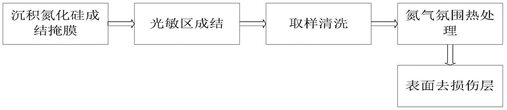
[0037] 1. Deposit silicon nitride diffusion mask 5, using plasma enhanced chemical vapor deposition (PECVD) technology to deposit silicon nitride junction mask 5 with a thickness of 200±30nm, the substrate temperature is 330±20°C, RF The power is 40±10W;

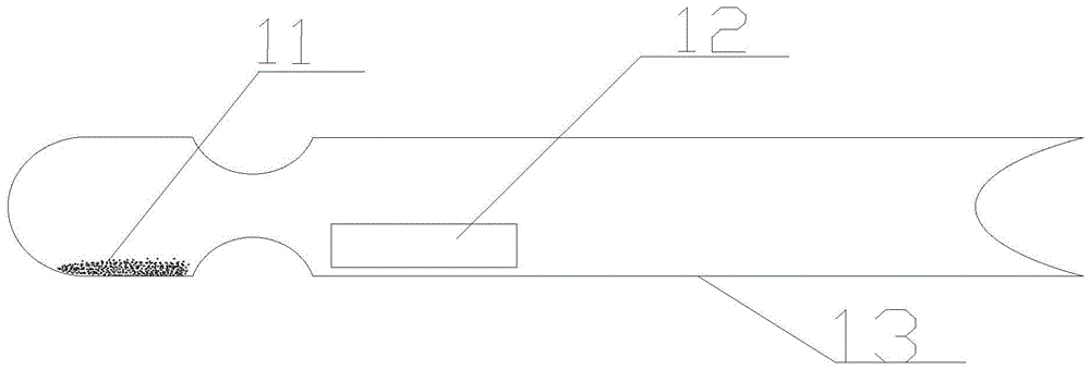
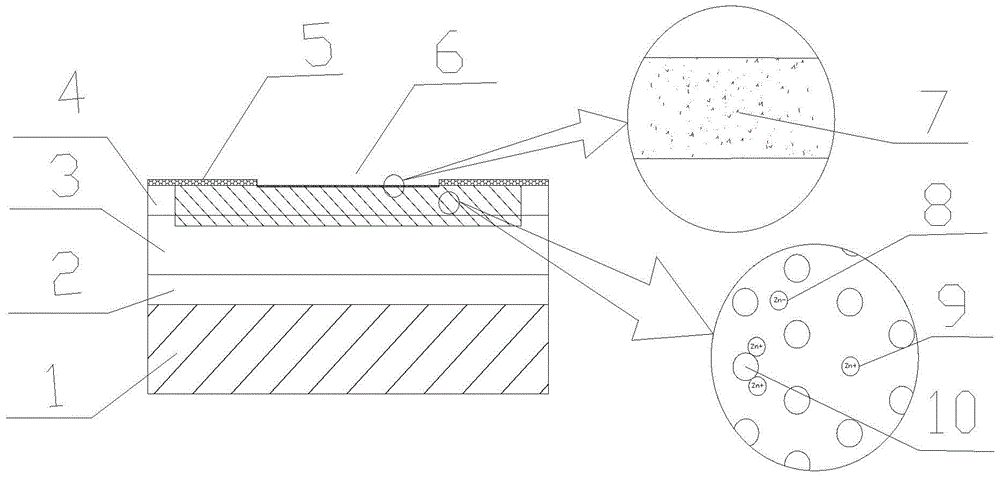
[0038] 2. First use the inductively coupled plasma (ICP) etching technology to open the window 6, and then put the element ion source 11 and the epitaxial wafer 12 into the source area and the sample area of ​​the quartz chamber 13 in sequence, such as figure 1 As shown, evacuate to 3×10 -4 Below Pa, then seal the quartz chamber 13, keep it at a temperature of 550±20°C for 9±3min, and then take it out quickly;

[0039] 3. Sampling and cleaning, opening the quartz chamber 13, taking out the epitaxial wafer 12, cleaning with chloroform, ether, acetone, and MOS grade ethanol, and drying with high-purity nitrogen.

[0040] 4. Heat treatment in a nitrogen atmosphere, put sample 12 into a thermal annealing furnace, maintain a n...

Embodiment 2

[0043] 1. Deposit silicon nitride diffusion mask 5, using plasma enhanced chemical vapor deposition (PECVD) technology to deposit silicon nitride junction mask 5 with a thickness of 200±30nm, the substrate temperature is 330±20°C, RF The power is 40±10W;

[0044] 2. First use the inductively coupled plasma (ICP) etching technology to open the window 6, and then put the element ion source 11 and the epitaxial wafer 12 into the source area and the sample area of ​​the quartz chamber 13 in sequence, such as figure 1 As shown, evacuate to 3×10 -4 Below Pa, then seal the quartz chamber 13, keep it at a temperature of 550±20°C for 9±3min, and then take it out quickly;

[0045] 3. Sampling and cleaning, opening the quartz chamber 13, taking out the epitaxial wafer 12, cleaning with chloroform, ether, acetone, and MOS grade ethanol, and drying with high-purity nitrogen.

[0046] 4. Heat treatment in a nitrogen atmosphere, put sample 12 into a thermal annealing furnace, maintain a n...

Embodiment 3

[0049] 1. Deposit silicon nitride diffusion mask 5, using plasma enhanced chemical vapor deposition (PECVD) technology to deposit silicon nitride junction mask 5 with a thickness of 200±30nm, the substrate temperature is 330±20°C, RF The power is 40±10W;

[0050] 2. First adopt the inductively coupled plasma (ICP) etching technology to open the window 6, and then put the element ion source 11 and the epitaxial wafer 12 into the source area and the sample area of ​​the quartz chamber 13 in sequence, such as figure 1 As shown, evacuate to 3×10 -4Below Pa, then seal the quartz chamber 13, keep it at a temperature of 550±20°C for 9±3min, and then take it out quickly;

[0051] 3. Sampling and cleaning, opening the quartz chamber 13, taking out the epitaxial wafer 12, cleaning with chloroform, ether, acetone, and MOS grade ethanol, and drying with high-purity nitrogen.

[0052] 4. Heat treatment in a nitrogen atmosphere. Put sample 12 into a thermal annealing furnace and maintain...


PUM


Abstract

The invention discloses a low-damage indium gallium arsenic detector p+n junction preparation method. The method comprises the following specific steps that: 1) silicon nitride junction formation mask deposition; 2) photosensitive area junction formation; 3) sampling and cleaning; 4) nitrogen atmosphere thermal treatment; and 5) surface damage layer removal. The nitrogen atmosphere thermal treatment, one the one hand, can restore lattice damage introduced in a junction formation process, reduce the density of recombination centers, and reduce the dark current of a detector, and on the other hand, can activate acceptor ions, decrease a donor compensation effect, increase hole carrier concentration in a P area, benefit the stability of P electrode ohmic contact and decrease series resistance; the surface damage layer removal, on the one hand, can effectively remove a surface oxidation layer, reduce recombination centers on a surface, benefit surface passivation, and improve the performance of the detector, and on the other hand, can remove an ion enrichment layer and a surface damage layer which are formed on the surface.

Description

technical field [0001] The invention relates to the preparation technology of infrared detectors, in particular to a low-damage InGaAs detector p + The n-junction preparation method is suitable for preparing high-performance short-wave infrared indium gallium arsenic detectors. Background technique [0002] In a near-room temperature environment, short-wave infrared InGaAs detectors have good performance, which makes them widely used in civil, military and aerospace fields. In the fabrication process of InGaAs shortwave infrared detector chip, p + The preparation of n-junction is one of the most critical processes. Because the junction process can bring relatively large damage to the chip, for short-wave infrared InGaAs detectors, optimizing the junction method plays a vital role in achieving high performance and high reliability. [0003] The cross-sectional structure of the InGaAs detector chip is as attached image 3 As shown, it consists of InP substrate 1, InP buffer...

Claims


Application Information

Patent Timeline
Patent Type & Authority Patents(China)
IPC IPC(8): H01L31/101H01L31/18
CPCH01L31/101H01L31/1844Y02P70/50
Inventor 曹高奇唐恒敬程吉凤石铭王瑞邵秀梅李庆法李雪龚海梅
Owner 无锡中科德芯感知科技有限公司
Why Eureka
Try Eureka