

Method for preparing lead selenide polycrystalline film on basis of oxygen ion beam assisted deposition
A technology of assisted deposition and oxygen ion beam, which is applied in the direction of chemical instruments and methods, ion implantation plating, polycrystalline material growth, etc., can solve the problems of CMOS process compatibility and limit the integration application of photosensitive arrays, and achieve the reduction of absorption defects, good Photoelectric properties and surface properties, effects of increased degrees of freedom
- Summary
- Abstract
- Description
- Claims
- Application Information
AI Technical Summary
Problems solved by technology
Method used
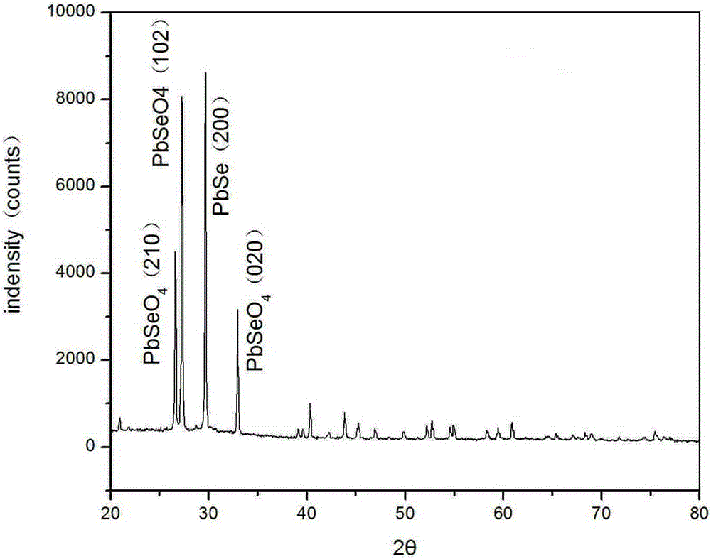
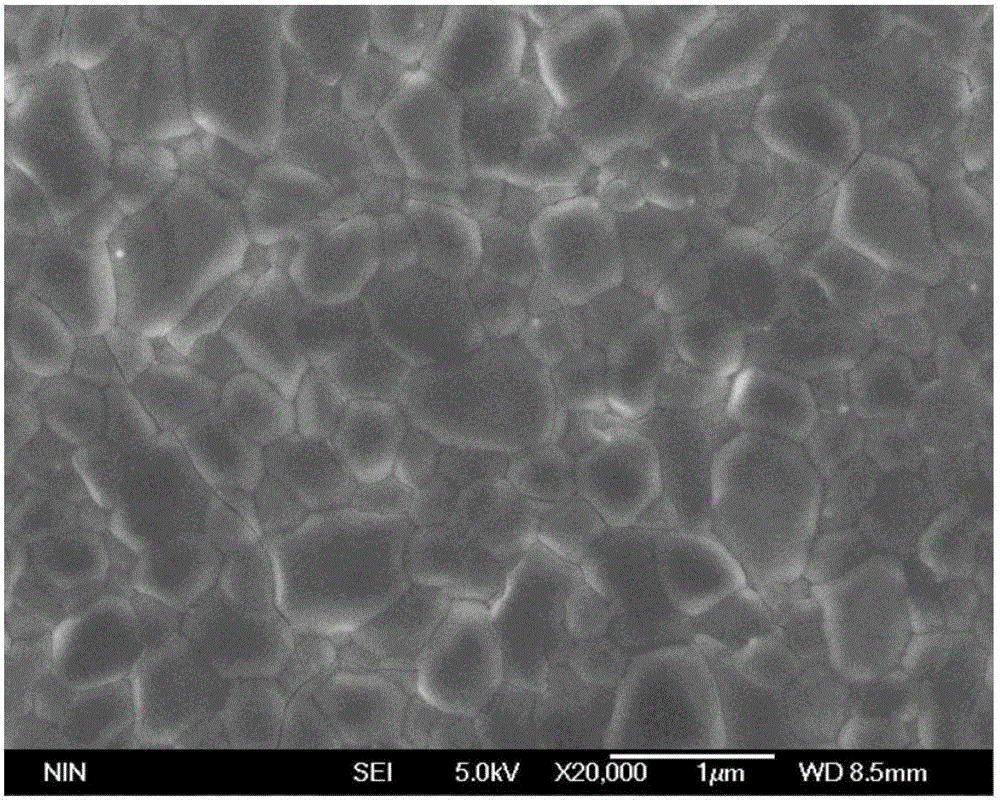
Image

Examples
Embodiment 1
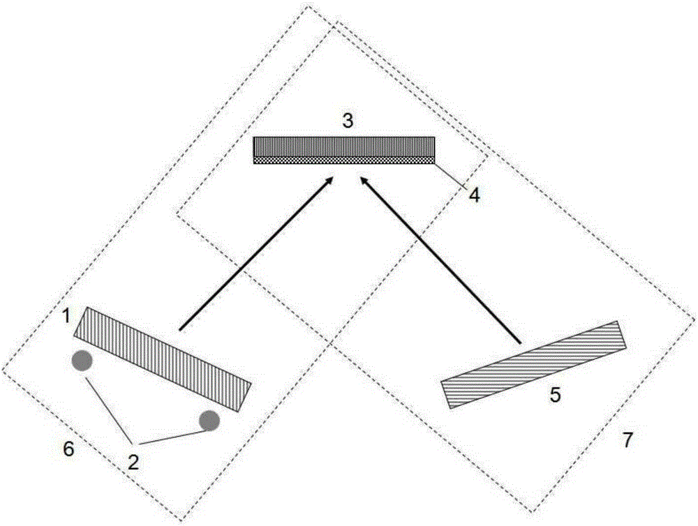
[0042] (1) The Si(100) substrate was ultrasonically cleaned for 15 min with absolute ethanol and acetone, and then washed with deionized water and dried for use. Si (100) substrate and PbSe powder (purity ≥ 99.99%) are respectively placed in the substrate frame 3 and the crucible 1 of the vacuum chamber, and the thermal evaporation system 6 is evacuated to 3 × 10 -4 Pa, and cover the substrate with a baffle. Increase the current of the heating source until the molecular beam evaporation rate reaches Reset the film thickness, remove the baffle, and start film growth with the substrate temperature stabilized at 120°C. When the thickness reaches 500nm, adjust the heating current to 0A and turn off the heating system to suspend the film growth. Start the ion source 5 to bombard the film with oxygen ions, the ion energy is 500eV, and the beam density is 100μA / cm 2 , the bombardment ends after 1 min. Use a baffle to block the film, and then increase the current of the heating s...
Embodiment 2
[0045] (1) The Si(100) substrate was ultrasonically cleaned for 15 min with absolute ethanol and acetone, and then washed with deionized water and dried for use. Si (100) substrate and PbSe powder (purity ≥ 99.99%) are respectively placed in the substrate frame 3 and the crucible 1 of the vacuum chamber, and the thermal evaporation system 6 is evacuated to 3 × 10 -4 Pa, and cover the substrate with a baffle. Increase the current of the heating source until the molecular beam evaporation rate reaches Reset the film thickness, remove the baffle, and start film growth with the substrate temperature stabilized at 120°C. When the film thickness reaches 1 μm, adjust the heating current to 0A and turn off the heating system to stop the film growth. Turn on the ion source 5, and the above-mentioned film is bombarded with oxygen ions, the ion energy is 500eV, and the beam current density is 100μA / cm 2 , the bombardment ends after 1 min.
[0046] (2) vacuum annealing is carried out...
Embodiment 3
[0048] (1) The Si(100) substrate was ultrasonically cleaned for 15 min with absolute ethanol and acetone, and then washed with deionized water and dried for use. Si (100) substrate and PbSe powder (purity ≥ 99.99%) are respectively placed in the substrate frame 3 and the crucible 1 of the vacuum chamber, and the thermal evaporation system 6 is evacuated to 3 × 10 -4 Pa, and cover the substrate with a baffle. Increase the current of the heating source until the molecular beam evaporation rate reaches Reset the film thickness, remove the baffle, and start film growth with the substrate temperature stabilized at 120°C. When the film thickness reaches 1 μm, adjust the heating current to 0A and turn off the heating system to stop the film growth. Turn on the ion source 5, and the above-mentioned film is bombarded with oxygen ions, the ion energy is 500eV, and the beam current density is 100μA / cm 2 , the bombardment ends after 1 min.
[0049] (2) The film obtained in the above ...
PUM
| Property | Measurement | Unit |
|---|---|---|
| thickness | aaaaa | aaaaa |
| thickness | aaaaa | aaaaa |
Abstract
Description
Claims
Application Information