Growing method for polycrystalline silicon carbide thin film

A polycrystalline silicon carbide and growth method technology, applied in ion implantation plating, metal material coating process, coating, etc., can solve the problem of poor density of silicon carbide film structure, large-scale application, cumbersome and complicated process, etc. problems, to achieve the effect of easy large-scale production, good compactness and good repeatability

Inactive Publication Date: 2016-05-04
XIAMEN UNIV
View PDF8 Cites 4 Cited by
  • Summary
  • Abstract
  • Description
  • Claims
  • Application Information

AI Technical Summary

Problems solved by technology

However, due to high manufacturing costs and some manufacturing process problems, it has been delayed in large-scale industrial application
[0003] At present, the industry mainly uses plasma-enhanced chemical vapor deposition (PECVD) as the preparation method when preparing silicon carbide films, and silane, methane and other gases are the main raw materials. The safety control in the production process is extremely strict and the process is complicated. Silicon carbide thin film has poor structural density
Chinese patent CN101985743A introduces a method of using plasma enhanced chemical vapor deposition (PECVD) to make a silico...

Method used


Image

  • Growing method for polycrystalline silicon carbide thin film
  • Growing method for polycrystalline silicon carbide thin film

Examples


Embodiment Construction

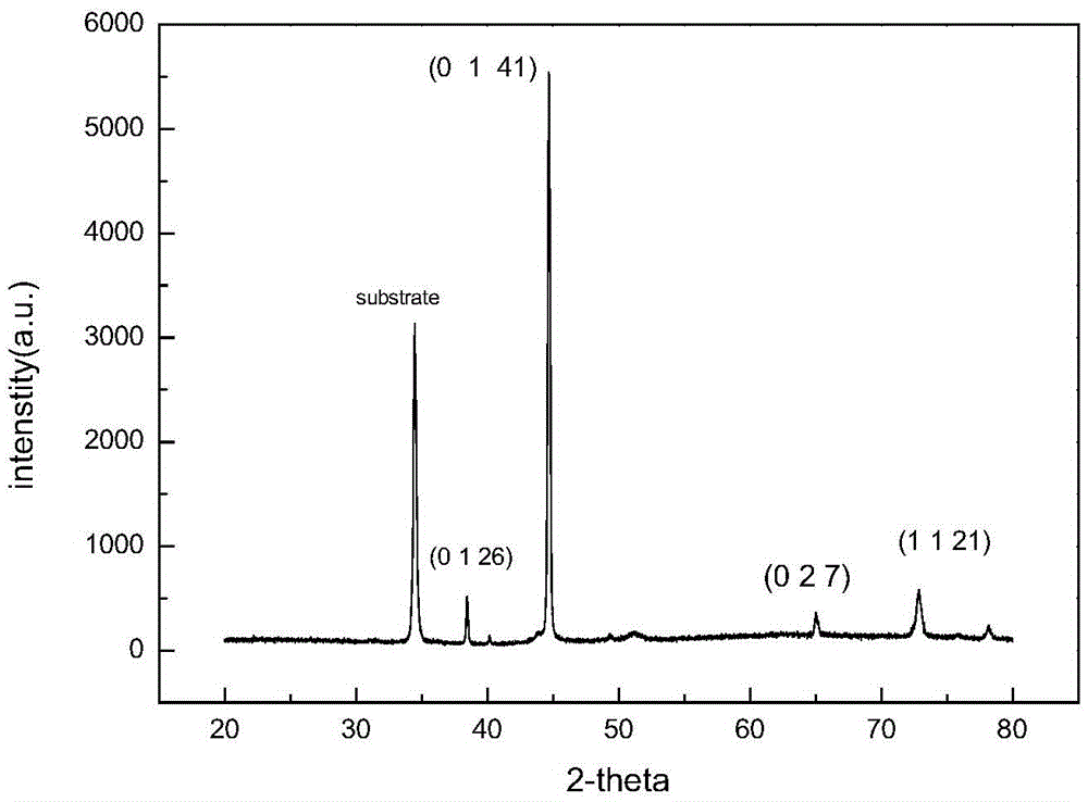
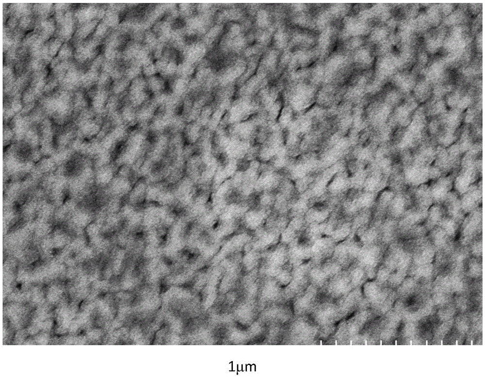
[0017] The process of preparing polycrystalline silicon carbide film by magnetron sputtering method is given below, including the following steps:

[0018] 1) Choose aluminum-doped zinc oxide as the substrate material, cut the sinking bottom into a 1cm×1cm square, put it in alcohol for ultrasonic cleaning for 15 minutes, and then put it in deionized water for ultrasonic cleaning for 5 minutes. Repeat this twice. in N 2 Blow dry under atmosphere. Choose silicon carbide as the target;

[0019] 2) Send the cleaned aluminum-doped zinc oxide substrate material into the magnetron sputtering apparatus, place the aluminum-doped zinc oxide substrate and the target in parallel, and then evacuate the magnetron sputtering chamber to a vacuum degree of 10 -5 Pa. Introduce argon gas with a flow rate of 120 sccm. And keep the air pressure in the magnetron sputtering chamber at 0.3Pa. After the air pressure is stable, turn on the RF AC power supply and adjust the power source so that th...


PUM


Abstract

The invention provides a growing method for a polycrystalline silicon carbide thin film, and relates to silicon carbide thin films. According to the growing method for the polycrystalline silicon carbide thin film, impurities and defects inside the silicon carbide thin film can be effectively reduced and overcome, the thin film rupture phenomenon caused by large tensile stress in the thin film is avoided, and the quality of the silicon carbide thin film is significantly improved. The growing method for the polycrystalline silicon carbide thin film comprises the steps that 1, a cleaned substrate is fed into a magnetron sputtering apparatus to be sputtered; 2, after sputtering is completed, cooling is conducted, so that an amorphous silicon carbide thin film sample is formed; and 3, after annealing is conducted, the polycrystalline silicon carbide thin film is obtained. A polycrystalline silicon carbide thin film sample is prepared on the aluminum-doped zinc oxide substrate through the magnetron sputtering apparatus. The silicon carbide thin film of uniform dimensions is obtained by controlling growth parameters. The preparation process is simple, the technology is stable, the repeatability is good and toxic or hazardous gases do not need to be used; in addition, the prepared polycrystalline silicon carbide thin film is high in deposition rate and good in compactness. The growing method for the polycrystalline silicon carbide thin film can be applied to the microelectronic industry and the photovoltaic industry and has the advantages of being low in cost, easy to produce in a large scale, free of pollution and the like.

Description

technical field [0001] The invention relates to a silicon carbide film, in particular to a method for growing a polycrystalline silicon carbide film. Background technique [0002] Silicon carbide powder has been widely used as abrasive since 1893. Sintering silicon carbide powder can produce hard ceramic-like silicon carbide particles, which can be used in materials that require high durability, such as automobile brake pads, clutches and bulletproof vests, in materials such as light-emitting diodes, early radio detectors, etc. It is also used in the manufacture of similar electronic devices. As a third-generation semiconductor material, silicon carbide has potential applications in high temperature, high frequency, high power, radiation resistance, and tool coating due to its wide band gap, high thermal conductivity, high critical breakdown electric field, and high hardness. And get the attention of photovoltaic, microelectronics, machinery industry [1-5] . When the dev...

Claims


Application Information

Patent Timeline
IPC IPC(8): C23C14/35C23C14/58C23C14/06
CPCC23C14/35C23C14/0635C23C14/5806
Inventor 张宇锋胡启涛林南英李晓军
Owner XIAMEN UNIV
Why Eureka
Try Eureka