Ultra-high-purity carbon nanotube conductive paste and preparation method thereof
A carbon nanotube and ultra-high-purity technology, applied in the field of preparation and modification of nanomaterials, can solve the problem of not seeing carbon nanotubes, etc., and achieve the effects of improving the utilization rate of raw materials, improving the catalytic efficiency, and eliminating potential safety hazards.
- Summary
- Abstract
- Description
- Claims
- Application Information
AI Technical Summary
Problems solved by technology
Method used
Image
Examples
preparation example Construction
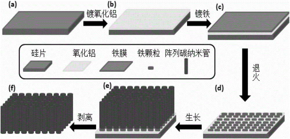
[0042] Another aspect of the present invention provides a method for preparing the above-mentioned ultra-high-purity carbon nanotube conductive paste, which includes the following steps:
[0043] (a) Select a single-sided polished silicon wafer, clean the surface of the silicon wafer and dry it, and deposit a layer of aluminum oxide film on the surface of the silicon wafer by reactive magnetron sputtering, the thickness of the aluminum oxide film is 10nm-60nm , the main component is aluminum oxide;
[0044] (b) using DC magnetron sputtering to deposit a layer of iron thin film catalyst on the surface of the aluminum oxide film, and the thickness range of the iron thin film catalyst is 1nm-3nm;
[0045] (c) Using water-assisted super growth method, the silicon chip with the iron thin film catalyst is put into a tube furnace for annealing, and the iron thin film catalyst on the surface of the silicon chip forms uniform iron nanoparticles, and under the assistance of moisture, th...
Embodiment 1
[0057] (1) Sonicate the silicon wafer polished on one side for 30 minutes in acetone to remove surface organic matter, then sonicate in ethanol for 30 minutes to remove surface particles, and finally dry it with nitrogen. At 25°C, set the RF sputtering power of 200w, the sputtering pressure of 11sccm, the ratio of argon to oxygen at 10, and react for 180s to obtain a 30nm thick aluminum oxide film.
[0058] (2) After reactive magnetron sputtering alumina, at 25°C, set 20w DC sputtering power, 12sccm sputtering pressure, and react for 15s to obtain a 1nm thick iron film.
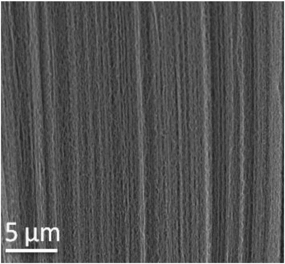
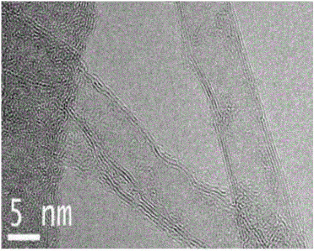
[0059] (3) At an annealing temperature of 750° C., anneal for 5 minutes, put the silicon wafer with the catalyst system in a tube furnace, anneal the iron film to form uniform nanoparticles, and have a moisture value of 150 ppm and an ethylene flow rate of 100 sccm , under the hydrogen flow rate of 700 sccm, grow for 15 minutes, and generate 100 μm arrayed carbon nanotubes on the surface of iron nanoparticles...
Embodiment 2
[0064] Example 1 was repeated with the same steps described above, the difference being that the sputtering time in step (2) was 20s.
PUM
| Property | Measurement | Unit |
|---|---|---|
| Diameter | aaaaa | aaaaa |
| Length | aaaaa | aaaaa |
| Thickness | aaaaa | aaaaa |
Abstract
Description
Claims
Application Information


