
Preparation method of ultrathin molybdenum disulfide nanosheet/silicon nanowire heterojunction structure

A technology of silicon nanowires and molybdenum disulfide, applied in chemical instruments and methods, chemical/physical processes, physical/chemical process catalysts, etc., can solve the problems of difficult large-scale application of catalysts, scarcity of precious metal resources, and low catalytic activity. Achieve the effect of increasing the density of catalytic active sites, unique light trapping, and good photocatalytic activity

Active Publication Date: 2018-01-12
INT ACAD OF OPTOELECTRONICS AT ZHAOQING SOUTH CHINA NORMAL UNIV
View PDF5 Cites 14 Cited by
  • Summary
  • Abstract
  • Description
  • Claims
  • Application Information

AI Technical Summary

Problems solved by technology

However, the inevitable weakness of silicon nanowires as a photocathode is its extremely low catalytic activity and poor stability in solution, so it is essential to load appropriate co-catalysts to improve its hydrogen evolution efficiency and stability.
Usually, noble metals such as platinum or their alloys are considered to be the best cocatalysts for the hydrogen evolution reaction, but due to the scarcity and high price of noble metal resources, it is difficult to realize large-scale application of such catalysts.

Method used


Image

  • Preparation method of ultrathin molybdenum disulfide nanosheet/silicon nanowire heterojunction structure
  • Preparation method of ultrathin molybdenum disulfide nanosheet/silicon nanowire heterojunction structure
  • Preparation method of ultrathin molybdenum disulfide nanosheet/silicon nanowire heterojunction structure

Examples


Embodiment 1

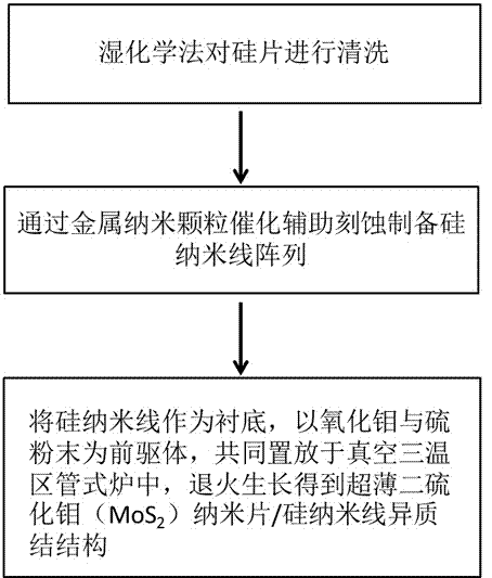
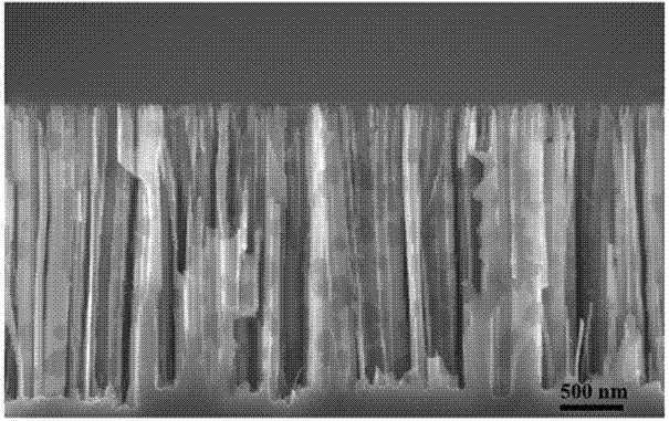
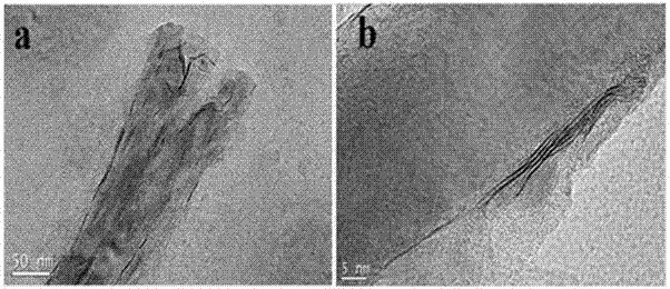
[0039] This application example provides a method for preparing ultra-thin molybdenum disulfide (MoS 2 ) method of nanosheet / silicon nanowire heterojunction structure material, the schematic diagram of the preparation process is as follows figure 2 , where (a) represents the silicon wafer after wet chemical cleaning; (b) represents the silicon nanowire array obtained by metal-assisted etching; (c) represents the ultra-thin molybdenum disulfide (MoS 2 ) nanosheet / silicon nanowire heterojunction structure.

[0040] Such as figure 1 As shown, the technical solution of the present invention is further described below.

[0041] (1) Cleaning of silicon wafers: Cut the P-type (100) oriented intrinsic silicon with a resistivity of 1~10Ω·cm on one side and cut it into 2×2 cm 2 Put the silicon wafer into acetone, ethanol, and deionized water for 10 minutes to remove the oil on the surface, then put it into a mixture of concentrated sulfuric acid and 40% hydrogen peroxide with a volum...

Embodiment 2

[0045] Test of Hydrogen Production Performance of Photoelectrocatalytic Water Splitting

[0046] The photoelectrocatalytic activity test and analysis was completed on a CHI660E electrochemical workstation, using a three-electrode test system. Silicon nanowires or ultrathin molybdenum disulfide (MoS 2 ) nanosheet / silicon nanowire heterojunction structure as the working electrode, the auxiliary electrode is a platinum wire electrode; the reference electrode is a saturated silver-silver chloride electrode. The electrolyte is a 0.5M sulfuric acid solution. 1 simulated sunlight for testing is achieved by using Xe lamps at 100mW / cm 2 realized under light.

[0047] Figure 6 It is the ultra-thin molybdenum disulfide (MoS) described in the present invention 2 ) Polarization curves of nanosheet / silicon nanowire heterojunction structure and pure silicon nanowire under light and dark conditions respectively, the applied bias voltage is -0.35~0.27V vs. s. From the data in the figur...


PUM

PropertyMeasurementUnit
Resistivityaaaaaaaaaa
Photocurrentaaaaaaaaaa

Abstract

The invention provides a preparation method of an ultrathin molybdenum disulfide nanosheet / silicon nanowire (SiNWs / MoS2) heterojunction structure. The preparation method comprises the following stepsthat S1, silicon wafers are cleaned; S2, the etching of a silicon nanowire array is assisted through the catalysis of metal nano particles; and S3, by taking the silicon nanowire array obtained in theS2 as a substrate, and molybdenum oxide and sulfur powder as a precursor, annealing growth is carried out, and the ultrathin molybdenum disulfide nanosheet / silicon nanowire heterojunction structure is obtained. Through the construction of the ultrathin molybdenum disulfide (MoS2) nanosheet / silicon nanowire heterojunction structure, the catalytic active site density of molybdenum disulfide can beimproved effectively, the photocatalysis hydrogen production efficiency of silicon nanowires is improved effectively and the catalysis stability of the silicon nanowires can be improved. A preparationprocess of the preparation method is simple and easy to implement, the cost is low, and mass production is easy.

Description

technical field [0001] The invention belongs to the technical field of new material preparation, and more specifically relates to a method for preparing an ultra-thin molybdenum disulfide nanosheet / silicon nanowire heterojunction structure. Background technique [0002] With the continuous growth of the global population, the non-renewability of fossil fuels and a series of environmental pollution problems caused by the combustion of fossil fuels, today's human beings are facing two major problems: energy crisis and environmental pollution. As a clean and high-energy-density new energy, hydrogen energy has attracted extensive attention from researchers in its development and application. The use of photocatalytic technology to split water to produce hydrogen is regarded as a potential ideal way to alleviate the energy crisis and reduce environmental pollution. [0003] Silicon, an earth-abundant and inexpensive semiconductor material with a relatively narrow bandgap (about ...

Claims


Application Information

Patent Timeline
IPC IPC(8): C25B11/06C25B1/04B01J27/051
CPCY02E60/36
Inventor 张璋胡蝶向杰程鹏飞王新
Owner INT ACAD OF OPTOELECTRONICS AT ZHAOQING SOUTH CHINA NORMAL UNIV
Learn More