Graphene preparation method

A technology of graphene and high-purity graphite, which is applied in the field of graphene, can solve the problems of long preparation time, difficulty in wide application, and high cost, and achieve the effects of improving surface smoothness, simple and easy process, and reducing formation temperature

Active Publication Date: 2018-06-26
NINGBO INST OF MATERIALS TECH & ENG CHINESE ACADEMY OF SCI
View PDF10 Cites 15 Cited by
  • Summary
  • Abstract
  • Description
  • Claims
  • Application Information

AI Technical Summary

Problems solved by technology

The graphene prepared by mechanical exfoliation method is of high quality, simple process, and the size reaches millimeter level, but the method takes a long time to prepare, the cost is high, and the number and size of graphene layers are uncontrollable, so it is difficult to be widely used; silicon carbide epitaxial growth method can prepare large Large-scale graphene, but silicon carbide is expensive, the preparation conditions are harsh, ultra-high vacuum is required, and the high temperature is above 1200°C; the graphene prepared by the graphite oxide reduction method has many defects; the most widely used method is chemical vapor deposition (CVD), which can realize Large-scale growth, but the carbon source of this method is carbon-containing gas, which requires pyrolysis (temperature 900 ° C ~ 1000 ° C), and there are many influencing factors, such as air pressure, flow rate, etc.

Method used


Image

  • Graphene preparation method
  • Graphene preparation method
  • Graphene preparation method

Examples


Embodiment 1

[0031] Step 1: The substrate Si is ultrasonically cleaned in an alcohol solution, and then dried.

[0032] Step 2: Depositing amorphous carbon film

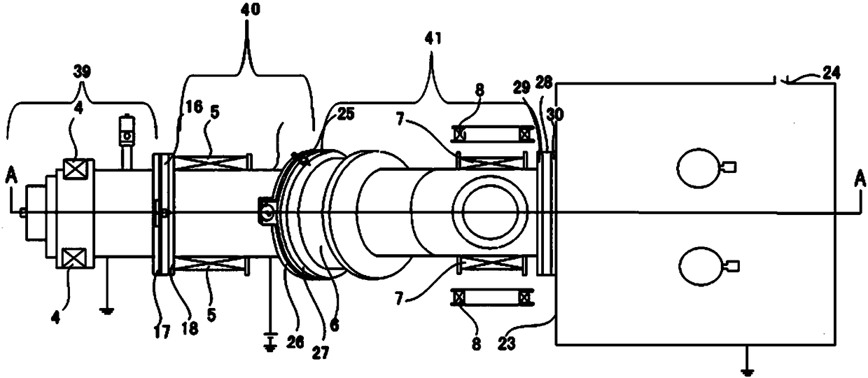
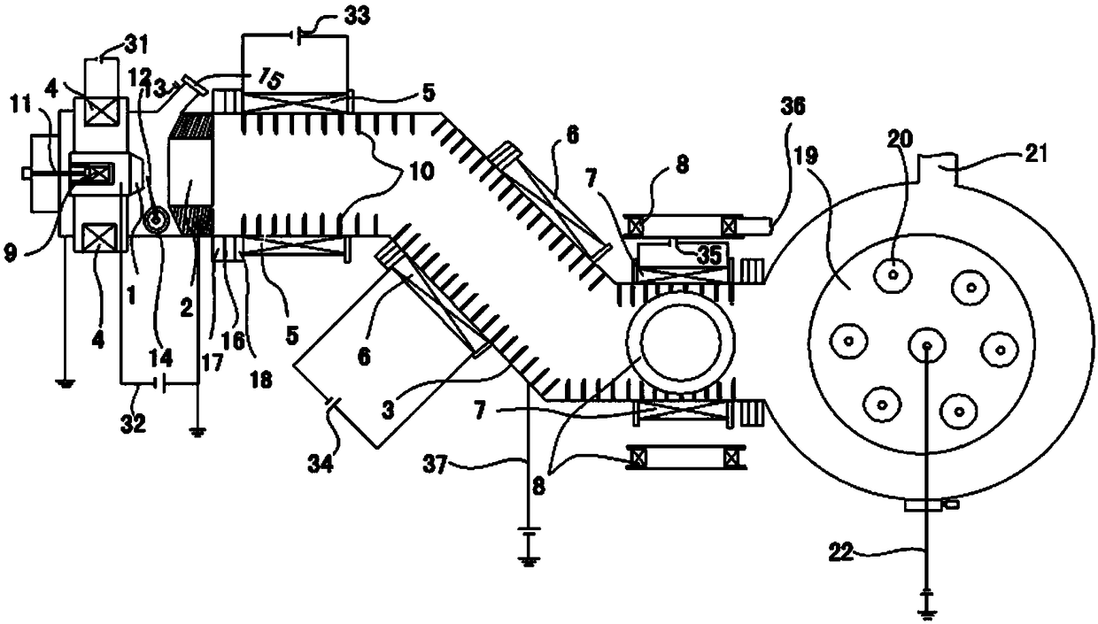
[0033] Using a cathode vacuum arc source film deposition device, the device structure is as figure 1 versus 2 As shown, it includes a cathode vacuum arc evaporation source 39, a magnetic filter part, and a thin film deposition vacuum chamber 23 installed with a substrate, which are sequentially sealed and connected.

[0034] Among them, the cathodic vacuum arc evaporation source 39 includes a trapezoidal cylindrical cathode 1, a cylindrical annular anode coaxial with the cathode 1, a trigger electrode 12 for igniting an arc, and a pneumatic trigger electrode 12 arranged between the cathode 1 and the anode 2. Valve 14. In this embodiment, the trigger electrode 12 is a pilot arc needle. The permanent magnet 9 and the anode 2 are coaxially placed on both sides of the cathode 1. The permanent magnet 9 is connected to a threaded rod 11. Sc...

Embodiment 2

[0051] Step 1: The substrate is the same as in Example 1, and the processing method is the same as Step 1 in Example 1;

[0052] Step 2: Depositing amorphous carbon film

[0053] It is basically the same as step 2 in embodiment 1, except that the coating conditions in step 2 are as follows:

[0054] Pass in argon gas 20sccm, arc current is 60A, elbow is applied with DC positive bias voltage of 10V, the magnitude of pulse negative bias voltage applied to the substrate is -100V, pulse frequency is 350KHz, and pulse width is 1.1μs;

[0055] Under the coating conditions for 8 min, the thickness of the deposited film is 15 nm.

[0056] Step 3: Same as step 3 in embodiment 1;

[0057] Step 4: Using a vacuum annealing furnace, the vacuum degree in the furnace reaches 3.0×10 -2 Pa. After the temperature reaches 450° C., the substrate Si after the above-mentioned vapor-deposited catalyst film is put into the substrate, kept for 20 minutes, and then air-cooled.

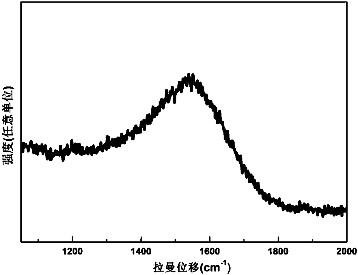
[0058] Raman spectroscopy was perfo...

Embodiment 3

[0060] Step 1: The substrate is the same as in Example 1, and the processing method is the same as Step 1 in Example 1;

[0061] Step 2: Depositing amorphous carbon film

[0062] It is basically the same as step 2 in embodiment 1, except that the coating conditions in step 2 are as follows: argon gas 20sccm, arc current 60A, elbow tube applies DC positive bias voltage 10V, substrate applies pulse negative bias voltage The size is -100V, the pulse frequency is 350KHz, and the pulse width is 1.1μs;

[0063] Under the coating conditions for 10 minutes, the thickness of the deposited film is 20 nm.

[0064] Step 3: Rinse the substrate Si after depositing the amorphous carbon film with a high-purity nitrogen gun and put it into a vacuum coating room. Use electron beam evaporation technology to prepare a copper catalyst film on the surface of the amorphous carbon film. The coating conditions are: pumping Vacuum to 2×10 - 3 Below Pa, set the electron gun power to 20W and the deposition rate...


PUM

PropertyMeasurementUnit
thicknessaaaaaaaaaa
surface roughnessaaaaaaaaaa
angleaaaaaaaaaa

Abstract

The invention provides a graphene preparation method, which combines a cathode vacuum electric arc deposition technology, an electron beam evaporation plating technology and a vacuum annealing process. According to the method, by optimizing process parameters, an amorphous carbon film with high sp3 content is deposited on the surface of a matrix, a catalyst film is subjected to evaporation platingat the surface through an electron beam, and finally annealing is performed at a temperature of 450-500 DEG C to diffuse and precipitate carbon onto the surface of the catalyst film so as to convertthe structure into the graphene structure to form the few-layer or multi-layer graphene. Compared to the existing graphene preparation process, the graphene preparation process of the invention has advantages of simpleness, easy performing, low annealing temperature and reduced cost; and the used carbon source is not the gas but the solid, and the number of the layers of graphene can be controlledby controlling the thickness of the carbon source so as to achieve the controlled preparation of graphene.

Description

Technical field [0001] The invention relates to the technical field of graphene, in particular to a preparation method for converting amorphous carbon into graphene. Background technique [0002] Graphene is made of sp 2 A two-dimensional atomic crystal with a hexagonal honeycomb crystal structure formed by the bonding of hybrid carbon atoms. Graphene is the basic unit constituting carbon nanotubes, fullerenes, and graphite bulk materials. [0003] In 2004, British scientists Novoselov and Geim used the micromechanical exfoliation method to obtain independent high-quality graphene, and discovered that graphene has unique electronic properties, thus setting off an upsurge in graphene research. Graphene has high carrier mobility and thermal conductivity, high light transmittance and good chemical stability. It has broad application prospects in many fields such as electronic devices, transparent electrode materials, energy storage materials, and functional composite materials. [000...

Claims


Application Information

Patent Timeline
Patent Type & Authority Applications(China)
IPC IPC(8): C01B32/184C23C14/32C23C14/30C23C14/06C23C14/18C23C14/58
CPCC01P2002/82C23C14/0605C23C14/18C23C14/30C23C14/325C23C14/5806
Inventor 汪爱英刘盼盼张栋郭婷李汉超柯培玲
Owner NINGBO INST OF MATERIALS TECH & ENG CHINESE ACADEMY OF SCI
Why Eureka
Try Eureka