Eureka AIR delivers breakthrough ideas for toughest innovation challenges, trusted by R&D personnel around the world.

A kind of thin film transistor and its preparation method and thin film transistor driving backplane

A technology of thin-film transistors and insulating films, which is applied in the direction of transistors, semiconductor/solid-state device manufacturing, semiconductor devices, etc., and can solve problems such as the inability to realize high-standard display backplanes, the performance degradation of short-channel devices, and the loss of the function of source and drain electrodes.

Active Publication Date: 2021-11-23
GUANG ZHOU NEW VISION OPTO ELECTRONICS TECH
View PDF6 Cites 0 Cited by
  • Summary
  • Abstract
  • Description
  • Claims
  • Application Information

AI Technical Summary

Problems solved by technology

It is easy to cause channel short circuit; 2. Chinese patent CN103094205B etc. introduce more oxygen vacancies through plasma bombardment, and oxygen vacancies act as donor defects to provide more carriers, but the formed oxygen vacancies may be in Under external conditions such as heating or light, self-healing occurs, and then the electrical conductivity decreases, losing the role of the source and drain electrodes. At the same time, the bombardment of the plasma may also cause the performance of short-channel devices to deteriorate, making it impossible to achieve high-standard display backplanes.

Method used


Image

  • A kind of thin film transistor and its preparation method and thin film transistor driving backplane
  • A kind of thin film transistor and its preparation method and thin film transistor driving backplane
  • A kind of thin film transistor and its preparation method and thin film transistor driving backplane

Examples


Embodiment 1

[0086] A method for preparing a metal oxide thin film transistor that suppresses the generation of parasitic capacitance, comprising the following steps in sequence:

[0087] In step a, a metal conductive layer is deposited and patterned on the substrate as a gate metal layer.

[0088] Before step a, silicon dioxide or silicon nitride can be pre-deposited on the transparent substrate as a buffer layer.

[0089] The metal used in the metal conductive layer is aluminum, copper, molybdenum, titanium, silver, gold, tantalum, tungsten, single chromium or aluminum alloy.

[0090] The metal conductive layer is a single-layer aluminum film, copper film, molybdenum film, titanium film, silver film, gold film, tantalum film, tungsten film, chromium film or aluminum alloy film, or two or more layers composed of the above single-layer metal films film.

[0091] The thickness of the metal conductive layer is set to 100nm to 2000nm; step b is entered after step a is completed.

[0092] I...

Embodiment 2

[0118] A method for preparing a metal oxide thin film transistor that suppresses the generation of parasitic capacitance, other steps are the same as in embodiment 1, the difference is that: between process steps d and e, there is also a step y, hydrophobic to the second insulating film The second insulating film having a hydrophobic layer is obtained by the chemical treatment.

[0119] Step y is specifically: spin-coat F-series polymer Cytop on the second insulating film to obtain a hydrophobic layer, F-series polymer Cytop is perfluorinated polymer Cytop or fluorocarbon polymer Cytop or AF cyclized fluorine At least one of the carbon polymer Cytop, the thickness of the hydrophobic layer is 5-20nm.

[0120] The preparation process of the thin film transistor of the present invention uses a self-alignment method to make an etching barrier layer, which maintains the structural characteristics of the bottom gate and the etching barrier layer, and can ensure the stability of the ...

Embodiment 3

[0125] A method for preparing a metal oxide thin film transistor that suppresses the generation of parasitic capacitance, comprising the following steps in sequence:

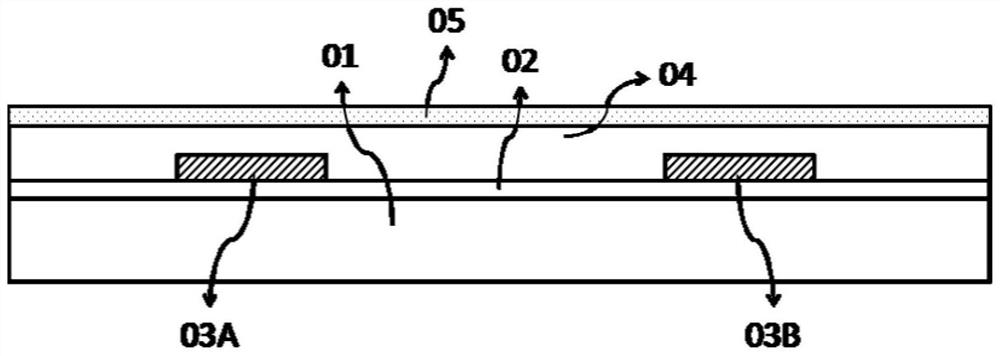
[0126] Such as figure 1 shown, in a SiO with 200nm thick 2 On the non-alkali glass substrate 01 of the buffer layer 02, a three-layer Mo / Al / Mo metal thin film is sequentially deposited by PVD (Physical Vapor Deposition) method, with thicknesses of 25nm / 100nm / 25nm respectively. It is patterned using a photolithography process to form a gate metal layer 03 .

[0127] It should be noted that the thickness of the gate metal layer is in the range of 100 nm to 2000 nm, and its specific size can be flexibly set according to actual needs, and is not limited to the size of this embodiment. The constituent material of the gate metal layer is also not limited to the case of this embodiment.

[0128] Such as figure 2 As shown, on the patterned gate metal layer 03, the PECVD method (Plasma Enhanced Chemical Vapor Depos...


PUM

PropertyMeasurementUnit
electrical resistivityaaaaaaaaaa
thicknessaaaaaaaaaa
thicknessaaaaaaaaaa

Abstract

A thin-film transistor and its preparation method and a thin-film transistor driving backplane. The preparation process of the thin-film transistor is based on the self-aligned exposure method to prepare an etching barrier layer, and uses a solution-level method instead of a plasma treatment method to prepare a conductive film. The problem of channel short circuit or reduced conductivity caused by plasma treatment is avoided. The preparation process of the present invention is simple, and the prepared thin film transistor has good stability, low parasitic capacitance and stable conductivity. Specifications, high precision, low-cost production.

Description

technical field [0001] The invention relates to the technical field of semiconductors, in particular to a metal oxide thin film transistor capable of suppressing generation of parasitic capacitance, a preparation method thereof, and a thin film transistor driving backplane. Background technique [0002] Thin Film Transistor (TFT, Thin Film Transistor) is an electrical switching thin film device, mainly used to control and drive liquid crystal display (LCD, Liquid Crystal Display), organic light-emitting diode (OLED, Organic Light-Emitting Diode) display sub-pixel, is One of the most important electronic devices in the field of flat panel displays. [0003] The film layers of the bottom-gate thin film transistor mainly include from bottom to top: gate, gate insulating layer, active layer, etch stop layer, source and drain electrodes, and subsequent passivation layer, leads and so on. If the coverage of the source-drain electrodes and the gate overlaps or overlaps in the vert...

Claims


Application Information

Patent Timeline
Patent Type & Authority Patents(China)
IPC IPC(8): H01L21/336H01L29/786H01L27/12
CPCH01L27/1214H01L29/66969H01L29/7869
Inventor 李民徐苗张伟周雷庞佳威王磊邹建华陶洪彭俊彪
Owner GUANG ZHOU NEW VISION OPTO ELECTRONICS TECH
Why Eureka
Eureka Blog
Learn More